C4304
C4304 is 2SC4304 manufactured by SavantIC.
.dat Sasaheveat4nu.tc Io Cm Semiconductor
Silicon NPN Power Transistors
Product Specification
2SC4304
DESCRIPTION
- With TO-220F package
- High voltage
- High speed switching
APPLICATIONS
- For switching regulator and general purpose applications
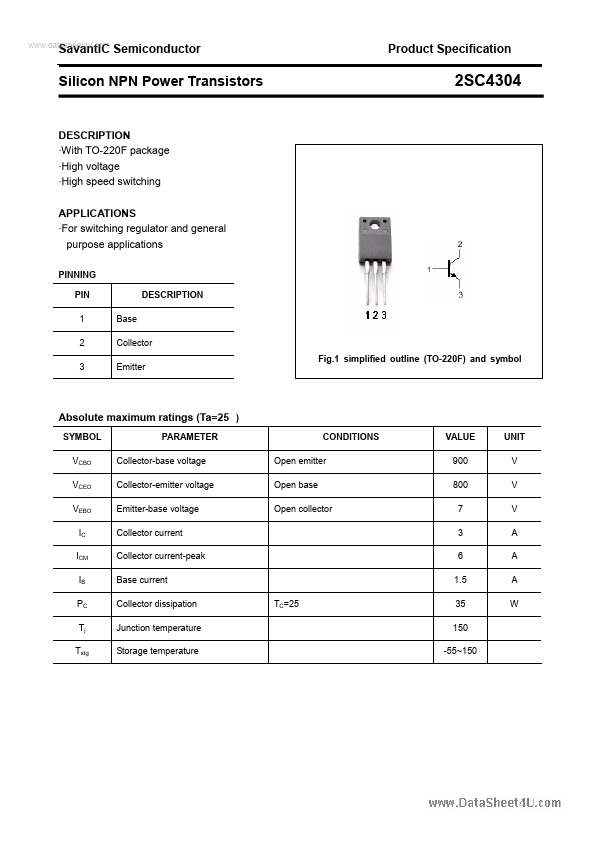
PINNING PIN 1 2 3
DESCRIPTION Base Collector Emitter
Fig.1 simplified outline (TO-220F) and...