Datasheet Summary
.datSasaheveat4nu.tcIoCm Semiconductor
Silicon NPN Power Transistors
Product Specification
2SC4517 2SC4517A
DESCRIPTION
- With TO-220F package
- High voltage switching transistor
APPLICATIONS
- For switching regulator and general purpose applications
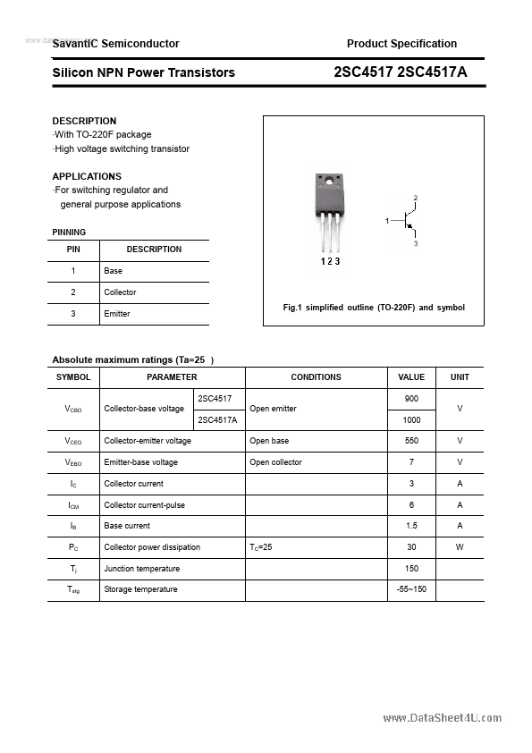
PINNING PIN 1 2 3
DESCRIPTION Base Collector Emitter
Fig.1 simplified outline (TO-220F) and...