2N6111 Overview
Description
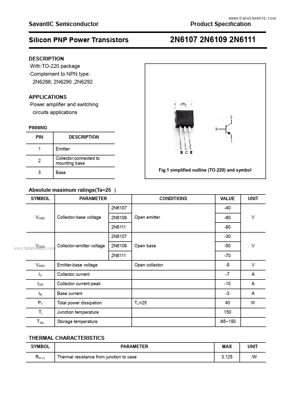
With TO-220 package - Complement to NPN type: 2N6288; 2N6290 ;2N6292 APPLICATIONS - Power amplifier and switching circuits applications PINNING PIN 1 2 3 DESCRIPTION Emitter Collector;connected to mounting base Base 2N6107 2N6109 2N6111 Fig.1 simplified outline (TO-220) and symbol SYMBOL PARAMETER 2N6107 VCBO Collector-base voltage 2N6109 2N6111 2N6107 CEO CONDITIONS VALUE -40 UNIT Open emitter -60 -80 -30 V V Collector-emitter voltage 2N6109 2N6111 Open base -50 -70 V VEBO IC ICM IB PT Tj Tstg Emitter-base voltage Collector current Collector current-peak Base current Total power dissipation Junction temperature Storage temperature Open collector -5 -7 -10 -3 V A A A W TC=25 40 150 -65~150 SYMBOL Rth j-c PARAMETER SavantIC Semiconductor Product Specification Silicon PNP Power Transistors CHARACTERISTICS Tj=25 unless otherwise specified PARAMETER 2N6107 VCEO(SUS) Collector-emitter sustaining voltage 2N6109 2N6111 VCEsat VBE Collector-emitter saturation voltage Base-emitter on voltage 2N6107 ICEO Collector cut-off current 2N6109 2N6111 2N6107 ICEX Collector cut-off current 2N6109 2N6111 IEBO Emitter cut-off current 2N6107 2N6109 2N6111 hFE-2 fT DC current gain Transition frequency IC=-7A;IB=-3A IC=-7A ; VCE=-4V VCE=-20V; IB=0 VCE=-40V; IB=0 VCE=-60V; IB=0 IC=-0.1A ;IB=0 SYMBOL 2N6107 2N6109 2N6111 CONDITIONS MIN -30 -50 -70 TYP. MAX UNIT V -3.5 -3.0 V V -1.0 mA VCE=-40V; VBE=-1.5V VCE=-30V; BE=-1.5V,TC=125 VCE=-60V; VBE=-1.5V VCE=-50V; BE=-1.5V,TC=125 VCE=-80V; VBE=-1.5V VCE=-70V; BE=-1.5V,TC=125 VEB=-5V; IC=0 IC=-2A ; VCE=-4V IC=-2.5A ; VCE=-4V IC=-3A ; VCE=-4V IC=-7A ; VCE=-4V IC=-0.5A ; VCE=-4V;f=1MHz 2.3 10 30 -0.1 -2.0 -0.1 -2.0 -0.1 -2.0 -1.0 mA mA hFE-1 DC current gain 150 MH.