Datasheet4U Logo Datasheet4U.com

S-89110A - MINI ANALOG SERIES CMOS OPERATIONAL AMPLIFIER

General Description

Non-inverted input pin GND pin Inverted input pin Output pin Positive power supply pin Internal Equivalent Circuit Figure 3  Figure 3 Figure 2 Figure 4 + 1 3 2 IN (+) VSS IN ( ) Figure 1 Internal Equivalent Circuit Output pin VDD Input pin VDD VSS Figure 2

Key Features

  • s y Lower operating voltage than the conventional general-purpose operational amplifiers: y Low current consumption: y Low input offset voltage: y Output full swing y Lead-free products VDD = 1.8 to 5.5 V IDD = 50 μA (S-89110A) IDD = 10 μA (S-89120A) 4.0 mV (max. ) y No external capaciters required for internal phase compensation.

📥 Download Datasheet

Full PDF Text Transcription (Reference)

The following content is an automatically extracted verbatim text from the original manufacturer datasheet and is provided for reference purposes only.

View original datasheet text
Rev.2.2_00 www.DataSheet4U.com MINI ANALOG SERIES CMOS OPERATIONAL AMPLIFIER S-89110A/89120A The mini-analog series is a group of ICs that incorporate a general purpose analog circuit in a small package. The S-89110A/89120A is a CMOS type single operational amplifier that has a phase compensation circuit, and that can be driven at a lower voltage with lower current consumption than existing bipolar operational amplifiers. These features make this product the ideal solution for small battery-powered portable equipment. The S-89110A/89120A is a single operational amplifier. „ 
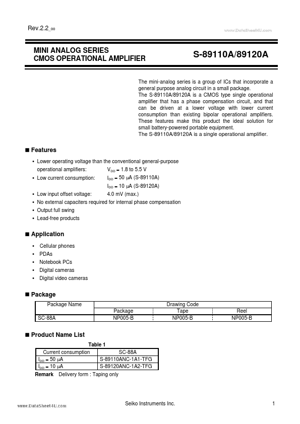
Features y Lower operating voltage than the conventional general-purpose operational amplifiers: y Low current consumption: y Low input offset voltage: y Output full swing y Lead-free products VDD = 1.8 to 5.