S-8204B Overview
Key Specifications
Package: TSSOP
Operating Voltage: 3.5 V
Max Voltage (typical range): 22 V
Min Voltage (typical range): 2 V
Key Features
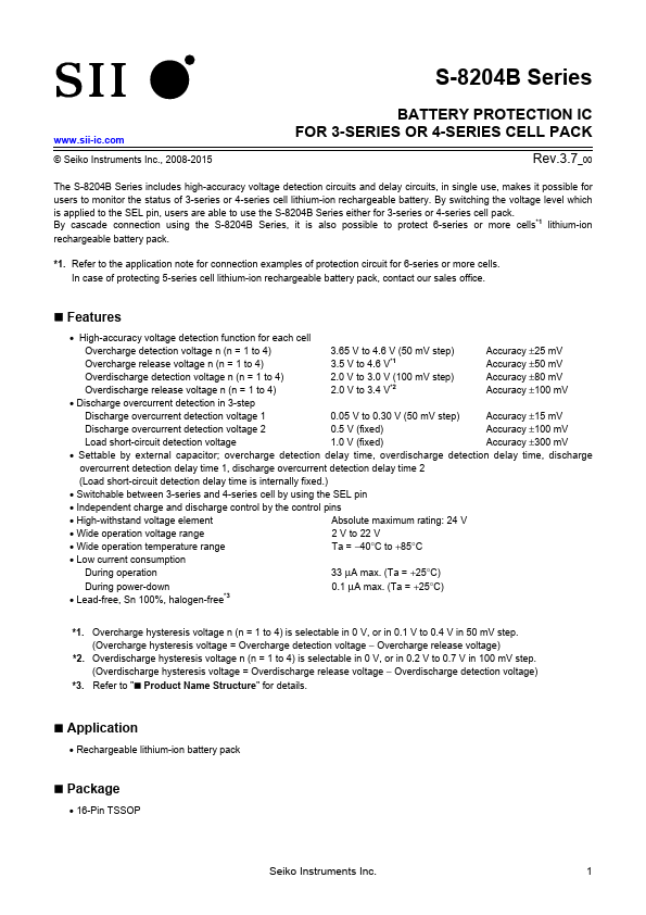
- High-accuracy voltage detection function for each cell Overcharge detection voltage n (n = 1 to
- Overcharge release voltage n (n = 1 to
- 3.65 V to 4.6 V (50 mV step) 3.5 V to 4.6 V*1 Accuracy ±25 mV Accuracy ±50 mV Overdischarge detection voltage n (n = 1 to
- Overdischarge release voltage n (n = 1 to
- 2.0 V to 3.0 V (100 mV step) 2.0 V to 3.4 V*2 Accuracy ±80 mV Accuracy ±100 mV
- Switchable between 3-series and 4-series cell by using the SEL pin
- Independent charge and discharge control by the control pins
- High-withstand voltage element

