S-8211D Overview
Key Specifications
Package: LSSOP
Operating Voltage: 1.8 V
Max Voltage (typical range): 8 V
Min Voltage (typical range): 1.5 V
Key Features
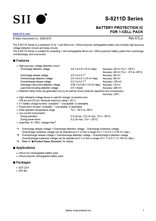
- Detection delay times are generated only by an internal circuit (external capacitors are unnecessary). Accuracy ±20%
- High-withstand voltage device is used for charger connection pins (VM pin and CO pin: Absolute maximum rating = 28 V)
- 0 V battery charge function "available" / "unavailable" is selectable
- Power-down function "available" / "unavailable" is selectable
- Wide operation temperature range Ta = -40°C to +85°C
- Low current consumption During operation 3.0 μA typ., 5.5 μA max. (Ta = +25°C) During power-down
- Lead-free, Sn 100%, halogen-free*3 0.2 μA max. (Ta = +25°C) *1. Overcharge release voltage = Overcharge detection voltage

