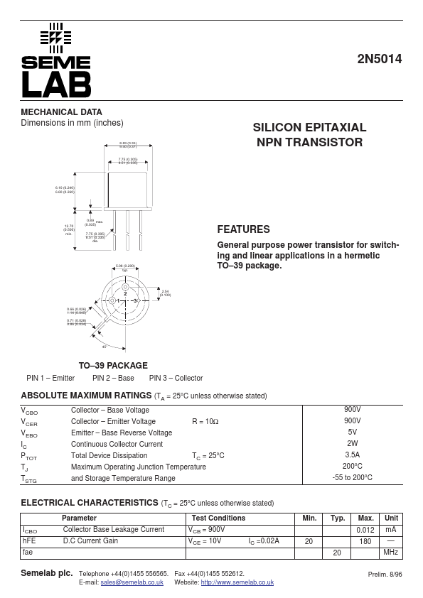
General purpose power transistor for switching and linear applications in a hermetic TO–39 package. 2 .5 4 (0 .1 0 0 ) 5 .0 8 (0 .2 0 0 ) ty p . 1 0 .6 6 (0 .0 2 6 ) 1 .1 4 (0 .0 4 5 ) 0 .7 1 (0 .0 2 8 ) 0 .8 6 (0 .0 3 4 ) 2 3 4 5 ° TO–39 PACKAGE PIN 1 – Emitter PIN 2 – Base PIN 3 – Collector
ABSOLUTE MAXIMUM RATINGS
(TA = 25°C unless otherwise stated) VCBO VCER VEBO IC PTOT TJ TSTG Collector – Base Voltage Collector – Emitter Voltage Emitter – Base Reverse Voltage Continuous Collector Current Total Device Dissipation and Storage Temperature Range TC = 25°C Maximum Operating Junction Temperature 900V R = 10W 900V 5V 2W 3.5A 200°C -55 to 200°C
This website uses cookies or similar technologies, to enhance your browsing experience and provide personalized recommendations. By continuing to use our website, you agree to our Privacy Policy