Seme LAB 2N7000CSM
N-channel MOSFET
| Part No. | 2N7000CSM |
|---|---|
| Datasheet | 2N7000CSM Download |
| Manufacturer |  Seme LAB |
| Description | N-channel MOSFET |
| Buy | Stock & Price |
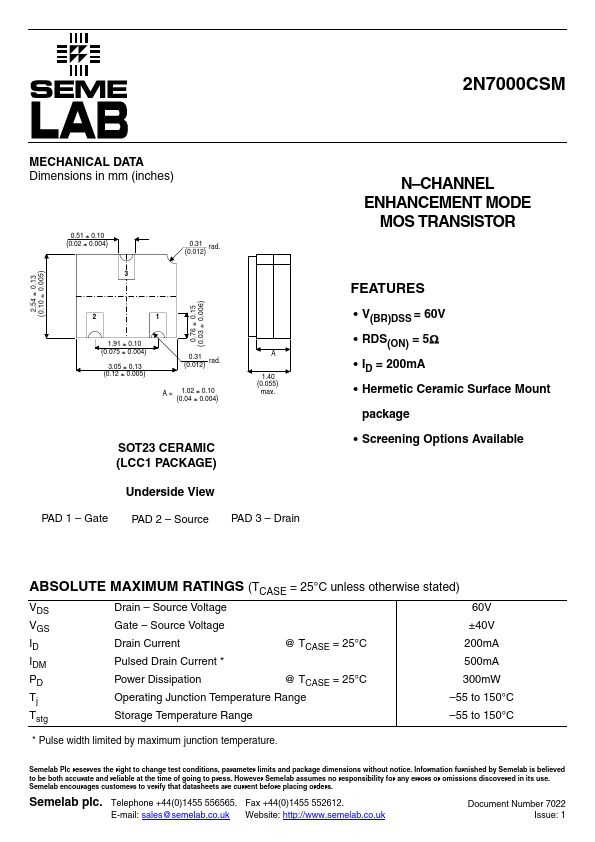
MECHANICAL DATA
Dimensions in mm (inches) 2.54 ± 0.13 (0.10 ± 0.005) 0.76 ± 0.15 (0.03 ± 0.006) 0.51 ± 0.10 (0.02 ± 0.004) 3 0.31 (0.012) rad. 2 1 1.91 ± 0.10 (0.075 ± 0.004) 3.05 ± 0.13 (0.12 ± 0.005) 0.31 (0.012) rad. A = 1.02 ± 0.10 (0.04 ± 0.004) A 1.40 (0.055) max. SOT23 CERAMIC (LCC1 PACKAGE) Underside View PAD 1 – Gate PAD 2 – Source PAD 3 – Drain N–CHANNEL ENHANCEMENT MODE MOS TRANSISTORFEATURES
● V(BR)DSS = 60V● RDS(ON) = 5Ω
● ID = 200mA
● Hermetic Ceramic Surface Mount package
● Screening Options Available
ABSOLUTE MAXIMUM RATINGS
(TCASE = 25°C unless otherwise stated) VDS Drain – Source Voltage 60V VGS Gate – Source Voltage ±40V ID Drain Current @ TCASE = 25°C 200mA IDM Pulsed Drain Current * 500mA PD Power Dissipation @ TCASE = 25°C 300mW Tj Operating Junction Temperature Range –55 to 150°C Tstg Storage Temperature Range –55 to 150°C * Pulse width limited by maximum junction temperature. Semelab Plc reserves the right to change test conditions, parameter limits and package dimensions without notice.