SML20W65
SML20W65 is N-CHANNEL ENHANCEMENT MODE HIGH VOLTAGE POWER MOSFETS manufactured by Seme LAB.
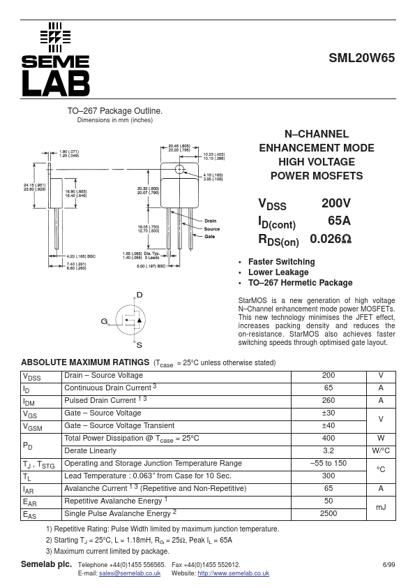
TO- 267 Package Outline.
Dimensions in mm (inches)
N- CHANNEL ENHANCEMENT MODE HIGH VOLTAGE POWER MOSFETS
VDSS 200V 65A ID(cont) RDS(on) 0.026Ω
- Faster Switching
- Lower Leakage
- TO- 267 Hermetic Package
Star MOS is a new generation of high voltage N- Channel enhancement mode power MOSFETs. This new technology minimises the JFET effect, increases packing density and reduces the on-resistance. Star MOS also achieves faster switching speeds through optimised gate layout.
ABSOLUTE MAXIMUM RATINGS (Tcase = 25°C unless otherwise stated)
VDSS ID IDM VGS VGSM PD TJ , TSTG TL IAR EAR EAS Drain
- Source Voltage Continuous Drain Current 3 Pulsed Drain Current 1 3 Gate
- Source Voltage Gate
- Source Voltage Transient Total Power Dissipation @ Tcase = 25°C Derate Linearly Operating and Storage Junction Temperature Range Lead Temperature : 0.063” from Case for 10 Sec. Avalanche Current 1 3 (Repetitive and Non-Repetitive) Repetitive Avalanche Energy 1 Single Pulse Avalanche Energy 2
1) Repetitive Rating: Pulse Width limited by maximum junction temperature. 2) Starting TJ = 25°C, L = 1.18m H, RG = 25Ω, Peak IL = 65A 3) Maximum current limited by package.
200 65 260 ±30 ±40 400 3.2
- 55 to 150 300 65 50 2500
V A A V W W/°C °C A m J
Semelab plc.
Telephone +44(0)1455 556565. Fax +44(0)1455 552612. Website: http://.semelab.co.uk E-mail: sales@semelab.co.uk
6/99
STATIC ELECTRICAL RATINGS (Tcase = 25°C unless otherwise stated)
BVDSS IDSS IGSS VGS(TH) ID(ON) RDS(ON) Characteristic Drain
- Source Breakdown Voltage Zero Gate Voltage Drain Current (VGS = 0V) Gate
- Source Leakage Current Gate Threshold Voltage On State Drain Current 2 4 Drain
- Source On State Resistance 2 Test Conditions VGS = 0V , ID = 250µA VDS = VDSS VDS = 0.8VDSS , TC = 125°C VGS = ±30V , VDS = 0V VDS = VGS , ID = 2.5m A VDS > ID(ON) x RDS(ON) Max VGS = 10V VGS = 10V , ID = 0.5 ID [Cont.] Test Conditions VGS = 0V VDS = 25V f = 1MHz VGS = 10V VDD = 0.5 VDSS ID = ID [Cont.] @ 25°C VGS = 15V...