VN10K-TO18
VN10K-TO18 is N-Channel MOSFET manufactured by Seme LAB.
..
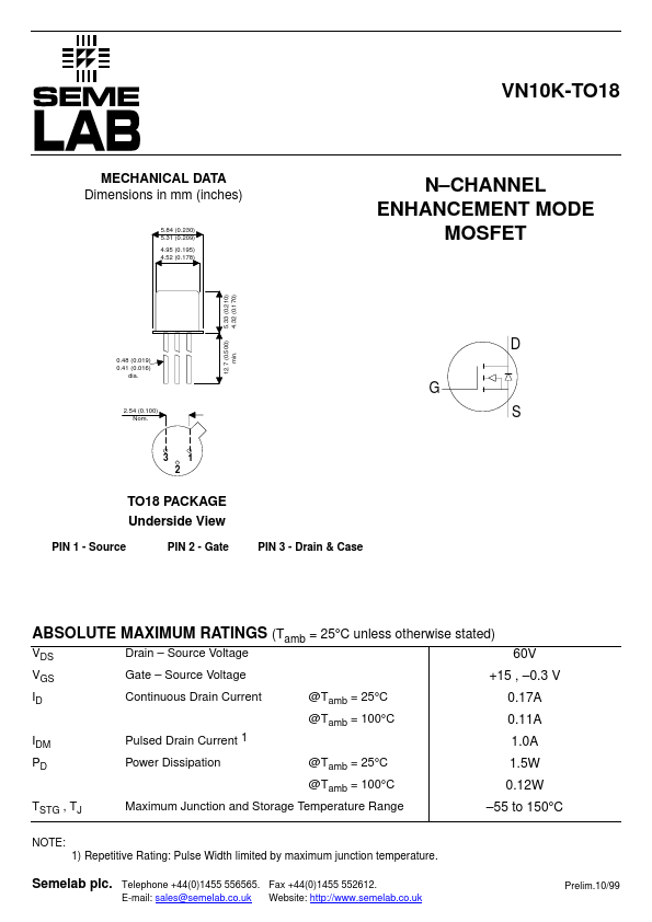
MECHANICAL DATA Dimensions in mm (inches)
5.84 (0.230) 5.31 (0.209) 4.95 (0.195) 4.52 (0.178)
N- CHANNEL ENHANCEMENT MODE MOSFET
5.33 (0.210) 4.32 (0.170)
0.48 (0.019) 0.41 (0.016) dia.
12.7 (0.500) min.
2.54 (0.100) Nom.
3 2 1
TO18 PACKAGE Underside View
PIN 1
- Source PIN 2
- Gate PIN 3
- Drain & Case
ABSOLUTE MAXIMUM RATINGS (Tamb = 25°C unless otherwise stated)
VDS VGS ID IDM PD TSTG , TJ
NOTE: 1) Repetitive Rating: Pulse Width limited by maximum junction temperature.
Drain
- Source Voltage Gate
- Source Voltage Continuous Drain Current Pulsed Drain Current 1 Power Dissipation @Tamb = 25°C @Tamb = 100°C Maximum Junction and Storage Temperature Range @Tamb = 25°C @Tamb = 100°C
60V +15 ,
- 0.3 V 0.17A 0.11A 1.0A 1.5W 0.12W
- 55 to 150°C
Semelab plc.
Telephone +44(0)1455 556565. Fax +44(0)1455 552612. E-mail: sales@semelab.co.uk Website: http://.semelab.co.uk
Prelim.10/99
ELECTRICAL RATINGS (Tamb = 25°C unless otherwise stated)
Characteristic BVDSS VGS(TH) IGSS IDSS ID(ON) RDS(ON) gfs gos Ciss Coss Crss ton toff STATIC CHARACTERISTICS Drain
- Source Breakdown Voltage Gate Threshold Voltage Gate
- Source Leakage Current Zero Gate Voltage Drain Current On State Drain Current 1 Static Drain
- Source On-State Resistance 1 Forward Transconductance 1 mon Source Output Conductance DYNAMIC CHARACTERISTICS Input capacitance Output capacitance Reverse transfer capacitance SWITCHING CHARACTERISTICS Turn- on Time Turn-off Time VDD = 15V ID = 0.6A VGEN = 10V Test Conditions VGS = 0V VDS = VGS VDS = 0V VDS = 48V VDS = 10V VGS = 5V VGS = 10V VDS = 10V VDS = 7.5V VGS = 0V VDS = 25V f = 1MHz RL = 23W ID = 100m A ID = 1m A VGS = 15V VGS = 0V TJ = 125°C VGS = 10V ID = 0.2A ID = 0.5A TJ = 125°C ID = 0.5A ID = 50m A 100 750 Min. 60 0.8 Typ. 120 1.4 1 0.7 3 1000 4 3 5.6 300 200 38 16 2 60 25 5 p F 7.5 5 9 m S 2.5 100 10 500 Max. Unit
V n A m A m A
W m S
RG = 25W
7 9
10 ns 10
NOTES: 1) Pulse Test: Pulse Width = 300ms , Duty Cycle £ 2%
THERMAL...