SemiHow HCD60R490
60V N-Channel Super Junction MOSFET
| Part No. | HCD60R490 |
|---|---|
| Datasheet | HCD60R490 Download |
| Manufacturer |  SemiHow |
| Description | 60V N-Channel Super Junction MOSFET |
| Buy | Stock & Price |
FEATURES
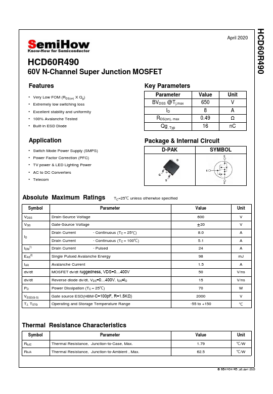
● Very Low FOM (RDS(on) X Qg)● Extremely low switching loss
● Excellent stability and uniformity
● 100% Avalanche Tested
● Built-in ESD Diode
KEY PARAMETERS
Parameter BVDSS @Tj,max ID RDS(on), max Qg, Typ Value 650 8 0.49 16 Unit V A Ω nC Application● Switch Mode Power Supply (SMPS)
● Power Factor Correction (PFC)
● TV power & LED Lighting Power
● AC to DC Converters
● Telecom Package & Internal Circuit D-PAK SYMBOL D G S
ABSOLUTE MAXIMUM RATINGS
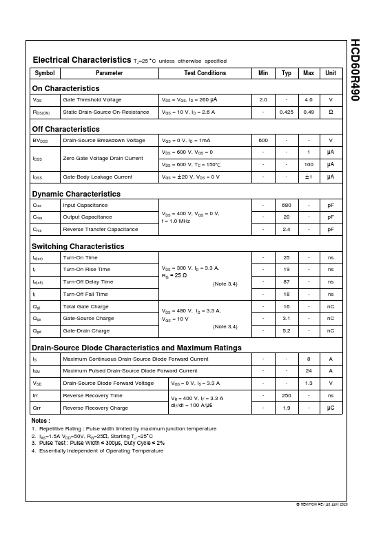
TC=25℃ unless otherwise specified Symbol VDSS VGS ID IDM1) EAS2) IAR dv/dt dv/dt PD VESD(G-S) TJ, TSTG Parameter Drain-Source Voltage Gate-Source Voltage Drain Current Drain Current Drain Current - Continuous (TC = 25℃) - Continuous (TC = 100℃) - Pulsed Single Pulsed Avalanche Energy Avalanche Current MOSFET dv/dt ruggedness, VDS=0…400V Reverse diode dv/dt, VDS=0…400V, IDS≤ID Power Dissipation (TC = 25℃) Gate source ESD(HBM-C=100pF, R=1.5KΩ) Operating and Storage Temperature Range Value 600 ±20 8.0 5.1 24 98 1.5 50 15 70 2000 -55 to +150 Unit V V A A A mJ A V/ns V/ns W V ℃ Thermal Resistance Characteristics Symbol RθJC RθJA Parameter Thermal Resistance, Junction-to-Case, Max.