SemiWell Semiconductor SFP730
This Power MOSFET is produced using SemiWell’s advanced planar stripe, DMOS technology. This latest technology has been especially designed to minimize on-state resistance, have a high rugged avalanche characteristics.| Part No. | SFP730 |
|---|---|
| Datasheet | SFP730 Download |
| Manufacturer |  SemiWell Semiconductor |
| Description | N-Channel MOSFET |
| Buy | Stock & Price |
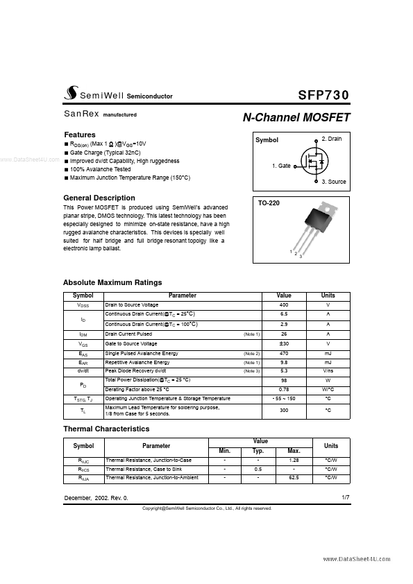
FEATURES
●● SFP730 N-Channel MOSFET Symbol ◀ {
●
● manufactured RDS(on) (Max 1 Ω )@VGS=10V Gate Charge (Typical 32nC) Improved dv/dt Capability, High ruggedness 100% Avalanche Tested Maximum Junction Temperature Range (150°C) { 2. Drain
●
●
●
● 1. Gate ▲ { 3. Source
GENERAL DESCRIPTION
This devices is specially well suited for half bridge and full bridge resonant topolgy like a electronic lamp ballast. TO-220 1 2 3ABSOLUTE MAXIMUM RATINGS
Symbol VDSS ID IDM VGS EAS EAR dv/dt PD TSTG, TJ TL Drain to Source Voltage Continuous Drain Current(@TC = 25°C) Continuous Drain Current(@TC = 100°C) Drain Current Pulsed Gate to Source Voltage Single Pulsed Avalanche Energy Repetitive Avalanche Energy Peak Diode Recovery dv/dt Total Power Dissipation(@TC = 25 °C) Derating Factor above 25 °C Operating Junction Temperature & Storage Temperature Maximum Lead Temperature for soldering purpose, 1/8 from Case for 5 seconds. (Note 2) (Note 1) (Note 3) (Note 1) Parameter Value 400 6.5 2.9 26 Units V A A A...