LH5324500
Key Features
- 3,145,728 words × 8 bit organization (Byte mode) 1,572,864 words × 16 bit organization (Word mode)
- Access time: 150 ns (MAX.)
- Power consumption: Operating: 357.5 mW (MAX.) Standby: 550 µW (MAX.)
- Static operation
- TTL compatible I/O
- Three-state outputs
- Single +5 V power supply
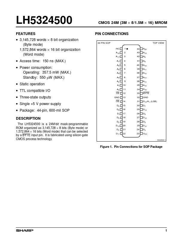
- Package: 44-pin, 600-mil SOP DESCRIPTION The LH5324500 is a 24M-bit mask-programmable ROM organized as 3,145,728 × 8 bits (Byte mode) or 1,572,864 × 16 bits (Word mode) that can be selected by a BYTE input pin. It is fabricated using silicon-gate CMOS process technology.