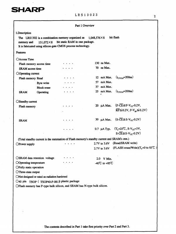
DESCRIPTION
memory and 131,072X8 It is fabricated using silicon-gate CMOS process technology. FEATURES
OAccess Time Flashmemoryaccesstime SRAM access time OOpemtingcurrent Flash memory Read Byte write Block erase SRAM ostandbycurrent bit flash - * * * . . . . . . . . . . . . . . . . - - * * 130 nsMax. 70 nsMax. 12 mAMax. 57 r&Max. 37 mAMax. 25 mA Max. , (t&ti2OOns) operatin% hcxJz.=2=) Flash memory . . . . 20 @ Max. (F-EZF-Vc,0.2V, EbO.2V, F-V&O.2V) (S-EZS-Vc,0.2V) (T,=25”c, S-V,-3V, S-CErs-Vcc-0.2V) Sk4M . . . . . . . . 30 pA Max. 0.7 @ Typ. (Total standby curnat is the summation of Flash memory’s standby current and SRAM’s one.) . . . . 2.7V to 3.6V @ead/SRAM write) OPower supply 2.7~ to 3.6~ @LASH erase/write)(T,=O to 85c OSRAM data retention voltage . . . . OOperating temperature OFully static operation oThree-state output 2.0 V Min. 40°C to +85”c ONot designed or rated as radiation hardened 040 pin TSOP ( TSOP~O-p-0819 plastic package OFlash memory has P-type bulk silicon, and SRAh4 has N-type bulk silicon. Sharp