FEATURES
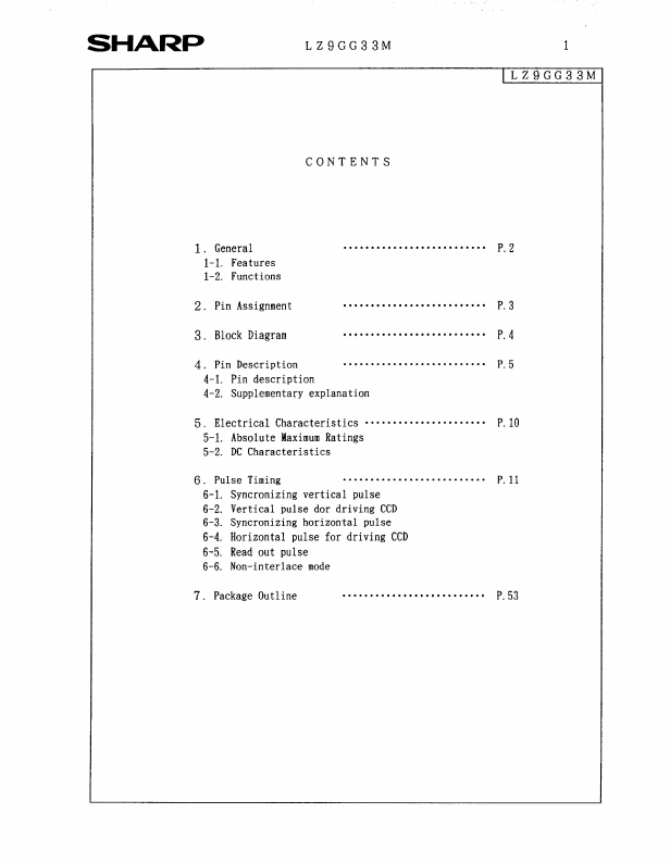
l-2. Functions Pin Assignment Block Diagram Pin DESCRIPTION
4-l. Pin description 4-2. Supplementary l t....**.*.~*****..~.*~... P. 2 2. 3. 4. . . . . . . . . . . . . . ..I.......... .**..****..*.*...........* ..,...****................ explanation l P. 3 P.4 P. 5 5. ELECTRICAL CHARACTERISTICS
5-L ABSOLUTE MAXIMUM RATINGS
5-2. DC Characteristics *.*..******....*..*.. P.10 ..*.***......,r***~......* 6 f Pulse Timing 6-l. Syncronizing vertical pulse 6-2. Vertical pulse dor driving CCD 6-3. Syncronizing horizontal pulse 6-4. Horizontal pulse for driving CCD 6-5. Read out pulse 6-6. Non-interlace mode 7. Package Outline . . ..+...*........****.*..* P. 11 P. 53 LZ9GG33M 1 LZ9GG33M 1. General is a CMOS gate array LSI. It generates timing pulses for pulse l-l. FEATURES
t * * t * t The package material is plastic. A p-type silicon circuit board is used. The process (structure) is CMOS. The delay time per 1 gate is 0.9ns. Not designed or rated as radiation hardened. 1-2. Functions Designed for CCD monochrome area sensor with 270,000 or 320,000 pixels. Sharp