PC925L0NUP0F
Overview
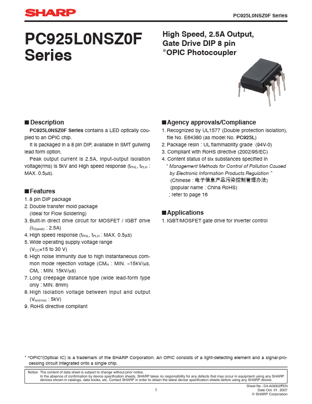
PC925L0NSZ0F Series contains a LED optically coupled to an OPIC chip. It is packaged in a 8 pin DIP, available in SMT gullwing lead form option.
- 8 pin DIP package
- Double transfer mold package (Ideal for Flow Soldering)
- Built-in direct drive circuit for MOSFET / IGBT drive (IO(peak) : 2.5A)
- High speed response (tPHL, tPLH : MAX. 0.5μs)
- Wide operating supply voltage range (VCC=15 to 30 V)
- High noise immunity due to high instantaneous com- mon mode rejection voltage (CMH : MIN. -15kV/μs, CML : MIN. 15kV/μs)
- Long creepage distance type (wide lead-form type only : MIN. 8mm)
- High isolation voltage between input and output (Viso(rms) : 5kV)
- RoHS directive compliant