FEATURES AND BENEFITS
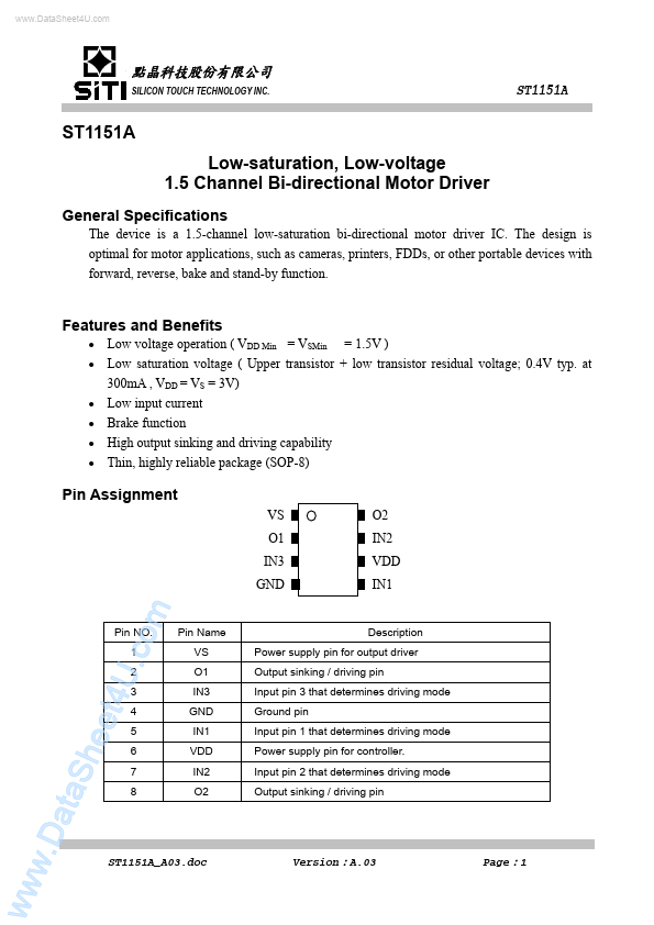
Low voltage operation ( VDD Min = VSMin = 1.5V ) Low saturation voltage ( Upper transistor + low transistor residual voltage; 0.4V typ. at 300mA , VDD = VS = 3V) Low input current Brake function High output sinking and driving capability Thin, highly reliable package (SOP-8) Pin Assignment VS O1 IN3 GND O2 IN2 VDD IN1 ww w.D ata Sh eet 4U .co m Pin NO. 1 2 3 4 5 6 7 8 Pin Name VS O1 IN3 GND IN1 VDD IN2 O2 DESCRIPTION
Power supply pin for output driver Output sinking / driving pin Input pin 3 that determines driving mode Ground pin Input pin 1 that determines driving mode Power supply pin for controller. Input pin 2 that determines driving mode Output sinking / driving pin ST1151A_A03.doc Version:A.03 Page:1 點晶科技股份有限公司 SILICON TOUCH TECHNOLOGY INC. ST1151A ABSOLUTE MAXIMUM RATINGS
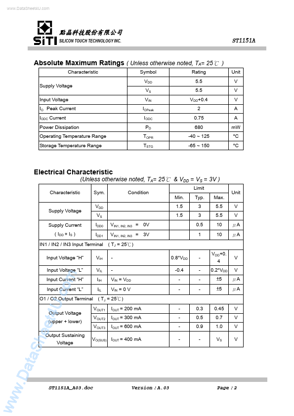
( Unless otherwise noted, TA= 25℃ ) Characteristic Supply Voltage Input Voltage IO Peak Current IODC Current Power Dissipation Operating Temperature Range Storage Temperature Range Symbol... SiTi