SiT1425B
SiT1425B is Active Resonator Drop-In Replacement manufactured by SiTime.
Features
- No load capacitors required
- No motional series resistance (ESR) pensation
- No negative resistance testing
- Guaranteed oscillator startup under all conditions
- One active resonator can drive up to two clock inputs
- All-inclusive frequency stability as low as ±20 ppm over extended temperature range (-55°C to 125°C)
- Fundamental frequencies between 115.2 MHz and
137 MHz accurate to 6 decimal places
- Industry best G-sensitivity of 0.1 ppb/g
- Low power consumption of 4.9 m A typical at 1.8 V
- LVCMOS patible output
- Industry-standard packages: 2.5 x 2.0, 3.2 x 2.5 mm x mm
- Ro HS and REACH pliant, Pb-free, Halogen-free and
Antimony-free
Conditions for Drop-In-Replacement
- Si T1425 is designed to work with non-wireless MCUs except for BLE which is supported
- Si T1425 is footprint patible to 4-pad SMD Xtal resonators with electrically grounded pin 2 and 4
- MCU/µC supports external oscillator mode
- MCU/µC supports GPIO output function on XTAL1 pin
(Figure 18) and able to drive ~6 m A across 1.8 V to 3.3 V VDD continuous voltage
Applications
- Ruggedized equipment in harsh operating environment
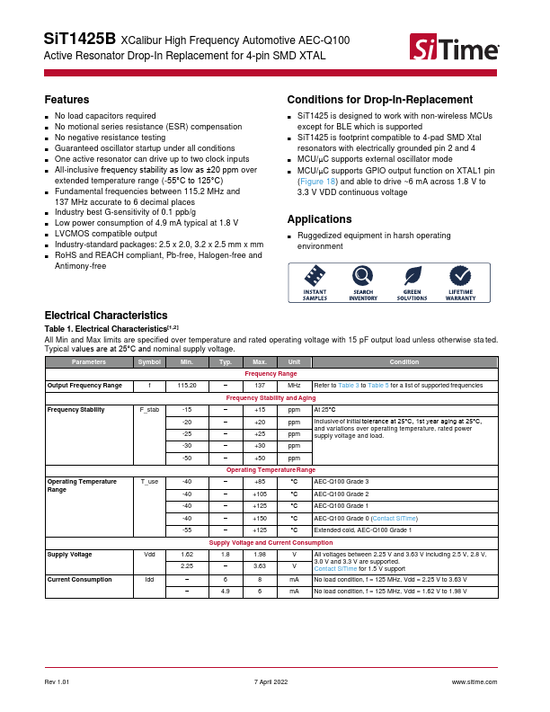
Electrical Characteristics
Table 1. Electrical Characteristics[1,2] All Min and Max limits are specified over temperature and rated operating voltage with 15 p F output load unless otherwise sta ted. Typical values are at 25°C and nominal supply voltage.
Parameters
Symbol
Min.
Typ.
Max.
Unit
Condition
Frequency Range
Output Frequency Range f
- 137
MHz Refer to Table 3 to Table 5 for a list of supported frequencies
Frequency Stability and Aging
Frequency Stability
F_stab...