BCR191S Overview
Key Features
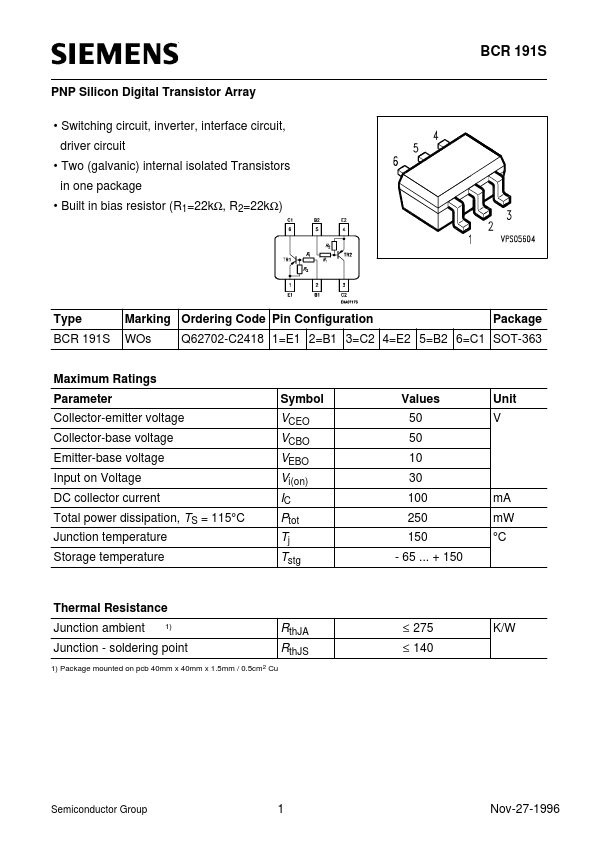
- Switching circuit, inverter, interface circuit, driver circuit
- Two (galvanic) internal isolated Transistors in one package
| Part | BCR191S |
|---|---|
| Description | PNP Silicon Digital Transistor Array (Switching circuit/ inverter/ interface circuit/ driver circuit) |
| Category | Transistor |
| Manufacturer | Siemens Semiconductor Group |
| Size | 43.91 KB |
| Part Number | Manufacturer | Description |
|---|---|---|
| BCR191S | Infineon | PNP Silicon Digital Transistor Array |
| BCR191 | Infineon | PNP Silicon Digital Transistor |
| BCR191W | Infineon | PNP Silicon Digital Transistor |
| BCR191F | Infineon | PNP Silicon Digital Transistor |
| BCR191T | Infineon | PNP Silicon Digital Transistor |