BSS139
SIPMOS® Small-Signal Transistor q q q q q q q
BSS 139
VDS 250 V ID 0.04 A RDS(on) 100 Ω
N channel Depletion mode High dynamic resistance Available grouped in VGS(th)
Type
Ordering Code
Tape and Reel Information
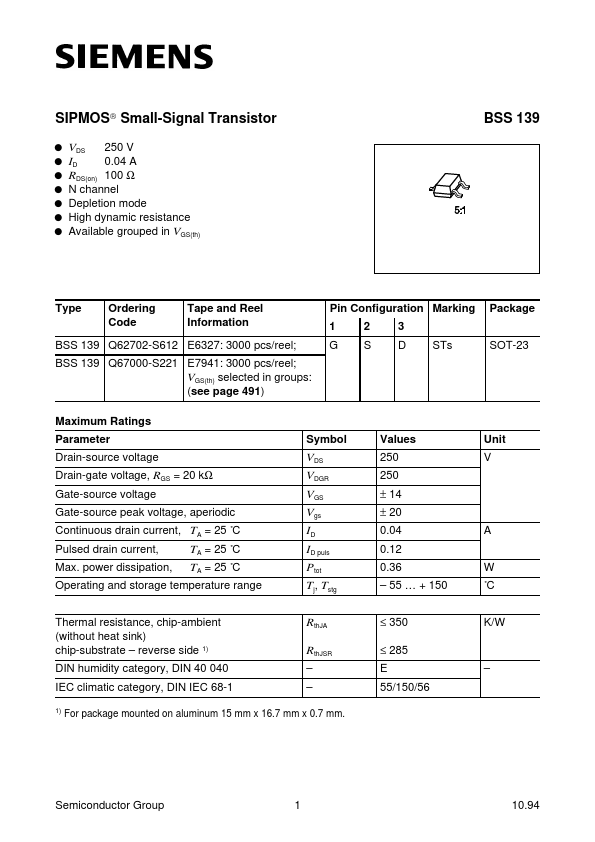
Pin Configuration Marking 1 G 2 S 3 D STs
Package SOT-23
BSS 139 Q62702-S612 E6327: 3000 pcs/reel; BSS 139 Q67000-S221 E7941: 3000 pcs/reel; VGS(th) selected in groups: (see page 491) Maximum Ratings Parameter Drain-source voltage Drain-gate voltage, RGS = 20 kΩ Gate-source voltage Gate-source peak voltage, aperiodic Continuous drain current, TA = 25 ˚C Pulsed drain current, Max. power dissipation,
Symbol
Values 250 250 ± 14 ± 20 0.04 0.12 0.36
- 55 … + 150 ≤ 350 ≤ 285 E 55/150/56
Unit V
TA = 25 ˚C TA = 25 ˚C
Operating and storage temperature range Thermal resistance, chip-ambient (without heat sink) chip-substrate
- reverse side 1) DIN humidity category, DIN 40 040 IEC climatic category, DIN IEC 68-1
1)
VDS VDGR VGS Vgs ID ID puls Ptot Tj, Tstg Rth JA Rth JSR
- -...