Datasheet4U.com
🌙
CFY77-10 Datasheet | Siemens Semiconductor Group
Part:
CFY77-10
Description:
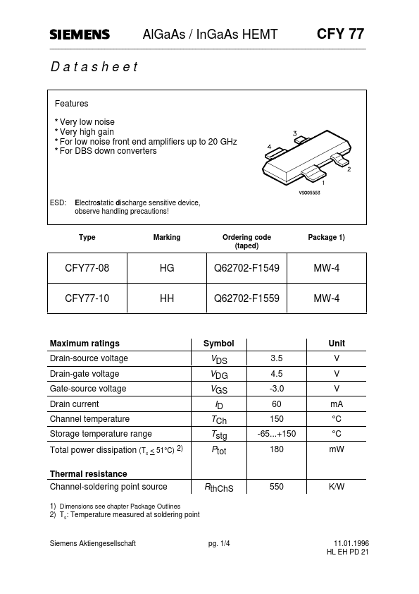
AlGaAs / InGaAs HEMT (Very low noise Very high gain For low noise front end amplifiers up to 20 GHz For DBS down converters)
Manufacturer:
Siemens Semiconductor Group
Size:
27.29 KB
CFY77-10 Datasheet (PDF) Download
Siemens Semiconductor Group
CFY77-10
×
Close