ILH100
Key Features
- Operating Temperature Range, -55°C to +125°C
- Current Transfer Ratio Guaranteed from -55°C to +100°C Ambient Temperature Range
- High Current Transfer Ratio at Low Input Current
- Isolation Test Voltage, 3000 VDC
- Base Lead Available for Transistor Biasing
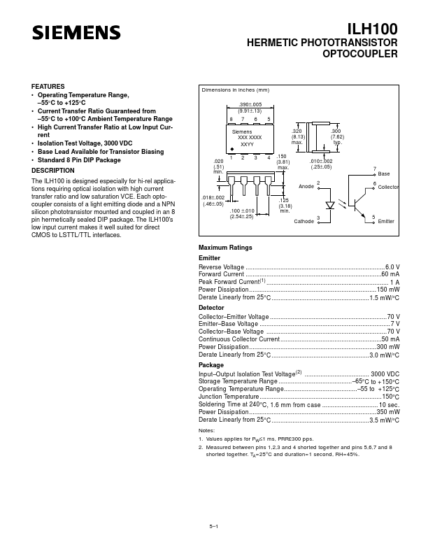
- Standard 8 Pin DIP Package DESCRIPTION The ILH100 is designed especially for hi-rel applications requiring optical isolation with high current transfer ratio and low saturation VCE. Each optocoupler consists of a light emitting diode and a NPN silicon phototransistor mounted and coupled in an 8 pin hermetically sealed DIP package. The ILH100's low input current makes it well suited for direct CMOS to LSTTL/TTL interfaces. Dimensions in inches (mm) .390±.005 (9.91±.13) 8 7 6 5 .320 (8.13) max. 4 .150 (3.81) max. .300 (7.62) typ. .010±.002 (.25±.05) 2 Siemens XXX XXXX XXYY .020 (.51) min. 1 2 3 7 Base 6 Anode .018±.002 (.46±.05) .100 ±.010 (2.54±.25) .125 (3.18) min. Cathode Collector 3 5 Emitter Notes:
- Values applies for PW≤1 ms, PRR£300 pps.
- Measured between pins 1,2,3 and 4 shorted together and pins 5,6,7 and 8 shorted together. TA=25°C and duration=1 second, RH=45%. 5-1 Characteristics (TΑ=25°C, unless otherwise specified) Parameter Emitter Forward Voltage Reverse Breakdown Voltage Reverse Current Capacitance Thermal Resistance Detector Collector-Emitter Saturation Voltage Base-Emitter Voltage Collector-Emitter Leakage Current DC Forward Current Gain Saturated DC Forward Gain Capacitance VCE(sat) VBE ICEO HFE HFE(sat) CCE CCB CEB RTH CTR(sat) CTEce Current Transfer Ratio, Collector-Base CTRcb Isolation and Insulation Common Mode Rejection Output High Common Mode Rejection Output High Package Capacitance Insulation Resistance Leakage Current, Input-Output CMH CML CIO RIO IIO 1011 1000 1000 2000 2000 1.5 1014 10 V/µs V/µs pF Ω µA VCM=500 Vp-p, VCC=5 V, RL=1 KΩ, IF=0 mA VCM=500 Vp-p, VCC=5 V, RL=1 KΩ, IF=10 mA VIO=0 V, 1 MHz VIO=500 VDC Relative Humidity ≤50%, VIO 3000 VDC, 5 sec. 0.4 0.7 0.9 % IF=10 mA, VCB=9.3 V 70 100 250 125 0.25 0.65 5 400 200 6.8 8.5 11 220 210 300 250 450 50 750 325 pF pF pF °C/W % % 0.4 V V nA IB=20µA, ICE=1 mA IB=20µA VCE=10 V VCE=10 V, IB=20µA VCE=0.4 V, IB=20µA VCE=5 V, f=1 MHz VF VBR IR CJ RTH 6 0.01 20 220 10 1.45 1.7 V V µA pF °C/W IF=60 mA IR=10 µA VR=6 V VF=0 V, f=1 MHz Junction to Lead Symbol Min. Typ. Max. Unit Condition Thermal Resistance Coupled Characteristics (-55°C to 100° C) Saturated Current Transfer Ratio Current Transfer Ratio, Collector-Emitter Junction to Lead IF=10 mA VCE=0.4 V IF=10 mA, VCE=10 V Typical Switching Speeds (TA=25°C) Non-Saturated Switching Delay Rise Storage Fall Propagation-High to Low Propagation-Low to High Saturated Switching(1) Delay Rise Storage Fall Propagation-High to Low Propagation-Low to High td tr ts tf tpHL tpLH 0.7 1 13.5 12 1.4 15 2 3 30 30 5 40 µs µs µs µs µs µs VCE=0.4 V VCE=0.4 V RL=1 KΩ IF=10 mA VCC=5 V, VTH=1.5 V RBE=open Symbol td tr ts tf tpHL tpLH Typ.
- 8 2 0.4 2 1 1.5 Max. 2 5 1.5 5 3 4 Unit µs µs µs µs µs µs Test Condition VCC=5 V RL=75 Ω IF=10 mA 50% of VPP RBE=open ILH100 5-2 Figure
- Switching time waveform and test schematic- non-saturated test condition Input IF 0 90% VOUT tr IF tf VCC 10% Pulse Width=100 µs Duty Cycle=1 % Figure