SFH6319T
SFH6319T is LOW CURRENT / HIGH GAIN OPTOCOUPLER manufactured by Siemens Semiconductor Group.
FEATURES
- Industry Standard SOIC-8 Surface Mountable Package
- High Current Transfer Ratio, 800%
- Low Input Current, 0.5m A
- High Output Current, 60m A
- Isolation Test Voltage, 2500 VACRMS
- TTL patible Output, VOL=0.1 V
- Adjustable Bandwidth-Access to Base
- Underwriters Lab File #E52744
- Available in Tape and Reel (suffix T) APPLICATIONS
- Logic Ground Isolation-TTL/TTL, TTL/CMOS, CMOS/CMOS, CMOS/TTL
- EIA RS 232C Line Receiver
- Low Input Current Line Receiver-Long Lines, Party Lines
- Telephone Ring Detector
- 117 VAC Line Voltage Status Indication-Low Input Power Dissipation
- Low Power Systems-Ground Isolation
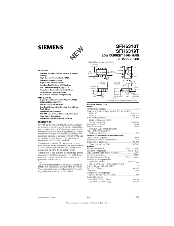
.240 (6.10)
Pin 1
.015±.002 (.38±.05)
7° .058±.005 (1.49±.13) .125±.005 (3.18±.13) Lead Coplanarity ±.0015 (.04 max.
.008 (.20)
5° max. R.010 (.25) max.
.021 (.53)
.050 (1.27) typ.
.020±.004 (.15±.10) 2 plcs.
TOLERANCE: ± .005 (unless otherwise noted)
DESCRIPTION
Very high current ratio together with 2500 VAC isolation are achieved by coupling an LED with an integrated high gain photodetector in a SOIC-8 package. Separate pins for the photodiode and output stage enable TTL patible saturation voltages with high speed operation. Photodarlington operation is achieved by tying the VCC and VO terminals together. Access to the base terminal allows adjustment to the gain bandwidth. The SFH6318T is ideal for TTL applications since the 300% minimum current transfer ratio with an LED current of 1.6 m A enables operation with one unit load-in and one unit load-out with a 2.2 KΩ pull-up resistor. The SFH6319T is best suited for low power logic applications involving CMOS and low power TTL. A 400% current transfer ratio with only 0.5 m A of LED current is guaranteed from 0°C to 70°C.
Caution: Due to the small geometries of this device, it should be handled with Electrostatic Discharge (ESD) precautions. Proper grounding would prevent damage further and/or degradation which may be induced by ESD.
Maximum Ratings (25°) Emitter Reverse Input...