HYB514265BJ-40
Description
Truth Table RAS H L L L L L L L L LCAS H H L H L L H L L UCAS H H H L L H L L L WE H H H H H L L L H OE H H L L L H H H H I/O1-I/O8 High-Z High-Z Dout High-Z Dout Din Don't care Din High-Z I/O9-I/O16 High-Z High-Z High-Z Dout Dout Don't care Din Din High-Z Operation Standby Refresh Lower byte read Upper byte read Word read Lower byte write Upper byte write Word write
Pin Names A0-A8 RAS UCAS, LCAS WE OE I/O1
- I/O16 Address Inputs Row Address Strobe Column Address Strobe Read/Write Input Output Enable Data Input/Output Power Supply: + 5 V for HYB 514265, + 3.3 V for HYB 314265 Ground (0 V) No Connection
N.C.
Semiconductor Group
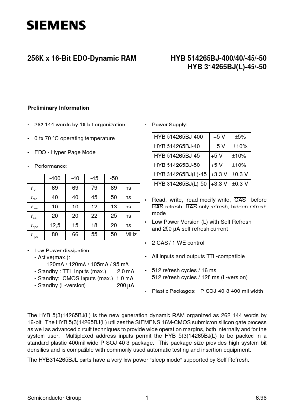
HYB 5(3)14265BJ(L)-400/-40/-45/-50 256K x 16 EDO-DRAM
Pin Configuration (top view)
P-SOJ-40-3
Semiconductor Group
HYB 5(3)14265BJ(L)-400/-40/-45/-50 256K x 16 EDO-DRAM
Block Diagram
Semiconductor Group
HYB 5(3)14265BJ(L)-400/-40/-45/-50 256K x 16 EDO-DRAM
Absolute Maximum Ratings Operating temperature range...