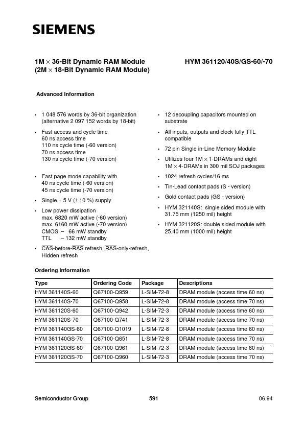
HYM361140GS-70
feature on the HYM 361120/40S/GS-60/-70 dictates the use of early write cycles.
Pin Definitions and Functions Pin No. A0-A9 DQ0-DQ35 CAS0
- CAS3 RAS0, RAS2 WE Function Address Inputs Data Input/Output Column Address Strobe Row Address Strobe Read/Write Input Power (+ 5 V) Ground Presence Detect Pin No Connection
VCC VSS
PD N.C.
Presence Detect Pins -60 PD0 PD1 PD2 PD3 -70
VSS VSS
N.C. N.C.
VSS VSS VSS
N.C.
Semiconductor Group
HYM 361120/40S/GS-60/-70 1M × 36-Bit
Pin Configuration (top view)
Semiconductor Group
HYM 361120/40S/GS-60/-70 1M × 36-Bit
Block Diagram Semiconductor Group 594
HYM 361120/40S/GS-60/-70 1M × 36-Bit
Absolute Maximum Ratings Operating temperature range 0 to + 70 ˚C Storage temperature range
- 55 to + 125 ˚C Soldering temperature...