HYS64V2200GU-8-3
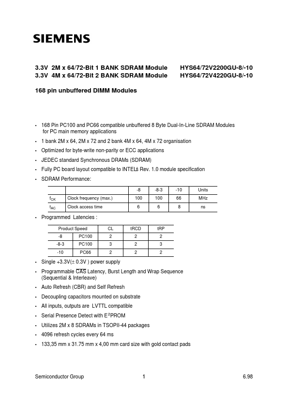
3.3V 2M x 64/72-Bit 1 BANK SDRAM Module 3.3V 4M x 64/72-Bit 2 BANK SDRAM Module 168 pin unbuffered DIMM Modules
HYS64/72V2200GU-8/-10 HYS64/72V4220GU-8/-10
- 168 Pin PC100 and PC66 patible unbuffered 8 Byte Dual-In-Line SDRAM Modules for PC main memory applications 1 bank 2M x 64, 2M x 72 and 2 bank 4M x 64, 4M x 72 organisation Optimized for byte-write non-parity or ECC applications JEDEC standard Synchronous DRAMs (SDRAM) Fully PC board layout patible to INTEL’ s Rev. 1.0 module specification SDRAM Performance:
-8 f CK t AC Clock frequency (max.) Clock access time 100 6 -8-3 100 6 -10 66 8 Units MHz ns
- -
- -
- -
Programmed Latencies :
Product Speed -8 -8-3 -10 PC100 PC100 PC66 CL 2 3 2 t RCD 2 2 2 t RP 2 3 2
- -
Single +3.3V(± 0.3V ) power supply Programmable CAS Latency, Burst Length and Wrap Sequence (Sequential & Interleave) Auto Refresh (CBR) and Self Refresh Decoupling capacitors mounted on substrate All inputs, outputs are LVTTL patible Serial Presence Detect with E...