Datasheet4U Logo Datasheet4U.com

SLG505YC264C - Clock Synthesizer

General Description

Pin # 1 2 3 4 Name PCI_0/CLKREQ_A# VDD_PCI PCI_1/CLKREQ_B# TME/PCI_2 Type I/O, SE PWR I/O, SE I/O, SE Description Configurable PCI clock output or CLKREQ input.

3.3V power supply for outputs.

Configurable PCI clock output or CLKREQ input.

Key Features

  • SLG505YC264C is fully compliant to Intel CK505 clock specification revision 1.0 SRC clocks compliant to PCI-Express Gen2 reference clock requirement (except SRC_0 and SRC_1) TME (Trusted Mode Enable) input to disable over-clocking support Two programmable single-ended outputs - 25MHz for LAN PHY with Wake-on-LAN support and 24.576MHz for 1394A controller 3.3 and low voltage (0.8V) I/O Power Supply Available in both commercial and industrial temperature ran.

📥 Download Datasheet

Datasheet Details

Part number SLG505YC264C
Manufacturer Silego
File Size 217.45 KB
Description Clock Synthesizer
Datasheet download datasheet SLG505YC264C Datasheet

Full PDF Text Transcription (Reference)

The following content is an automatically extracted verbatim text from the original manufacturer datasheet and is provided for reference purposes only.

View original datasheet text
SLG505YC264C Clock Synthesizer for Intel PCI-Express Gen2 Chipset
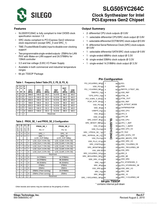
 Features • • • • SLG505YC264C is fully compliant to Intel CK505 clock specification revision 1.0 SRC clocks compliant to PCI-Express Gen2 reference clock requirement (except SRC_0 and SRC_1) TME (Trusted Mode Enable) input to disable over-clocking support Two programmable single-ended outputs - 25MHz for LAN PHY with Wake-on-LAN support and 24.576MHz for 1394A controller 3.3 and low voltage (0.8V) I/O Power Supply Available in both commercial and industrial temperature ranges 64 pin TSSOP Package Output Summary • • • • • • • • 2- differential CPU clock outputs @ 0.8V 1 - selectable differential CPU/SRC clock output @ 0.8V 1 - selectable differential DOT96/SRC clock output @ 0.