CY28354-400
CY28354-400 is 210MHz 24 Output Buffer manufactured by Silicon Labs.
210 MHz 24 Output Buffer for 4-DDR DIMMS for VIA Chipsets Support
Features
Functional Description
- Supports VIA PRO 266, KT266 and P4x266
- Dual 1- to 12-output buffer/driver
- Supports up to four DDR DIMMs
- Low-skew outputs (< 75 ps)
- Supports 266-MHz, 333-MHz and 400-MHz DDR SDRAM
- SMBus Read and Write support
- Space-saving 48-pin SSOP package
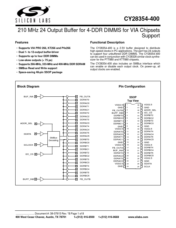
The CY28354-400 is a 2.5V buffer designed to distribute high-speed clocks in PC applications. The part has 24 outputs to support four unbuffered DDR DIMMS. The CY28354-400 can be used in conjunction with CY28326 similar clock synthesizer for the PTT880 and KTT880 chipsets.
The CY28354-400 also includes an SMBus interface which...