CY2SSTV857-27
Description
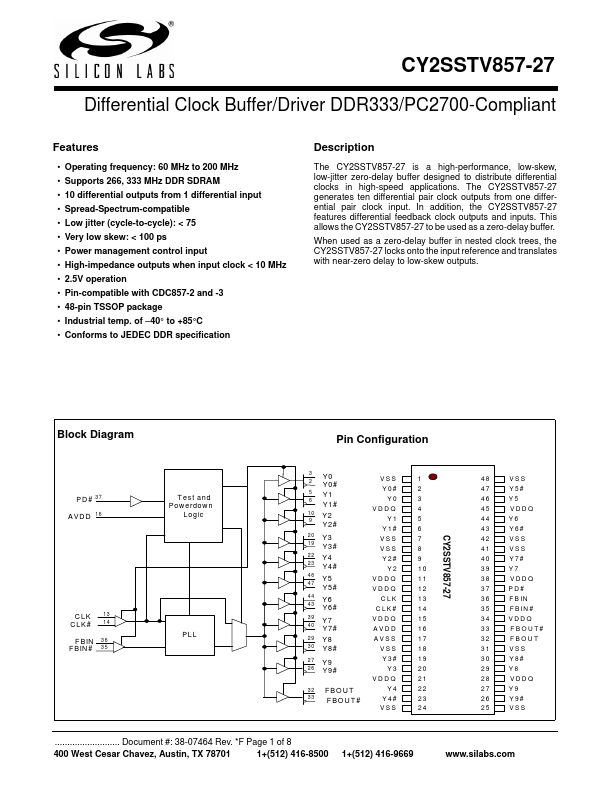
The CY2SSTV857-27 is a high-performance, low-skew, low-jitter zero-delay buffer designed to distribute differential clocks in high-speed applications. The CY2SSTV857-27 generates ten differential pair clock outputs from one differential pair clock input.
Key Features
- Operating frequency: 60 MHz to 200 MHz
- Supports 266, 333 MHz DDR SDRAM
- 10 differential outputs from 1 differential input
- Spread-Spectrum-compatible
- Low jitter (cycle-to-cycle): < 75
- Very low skew: < 100 ps
- Power management control input
- High-impedance outputs when input clock < 10 MHz
- 2.5V operation
- Pin-compatible with CDC857-2 and -3