SL18861DI
Overview
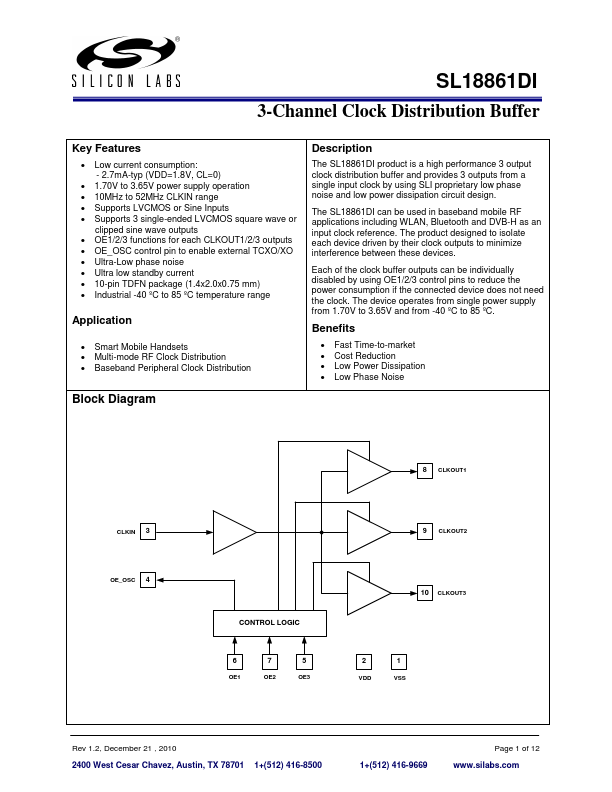
The SL18861DI product is a high performance 3 output clock distribution buffer and provides 3 outputs from a single input clock by using SLI proprietary low phase noise and low power dissipation circuit design. The SL18861DI can be used in baseband mobile RF applications including WLAN, Bluetooth and DVB-H as an input clock reference.
- Low current consumption: - 2.7mA-typ (VDD=1.8V, CL=0)
- 1.70V to 3.65V power supply operation
- 10MHz to 52MHz CLKIN range
- Supports LVCMOS or Sine Inputs
- Supports 3 single-ended LVCMOS square wave or clipped sine wave outputs
- OE1/2/3 functions for each CLKOUT1/2/3 outputs
- OE_OSC control pin to enable external TCXO/XO
- Ultra-Low phase noise
- Ultra low standby current
- 10-pin TDFN package (1.4x2.0x0.75 mm)