DESCRIPTION
Power MOSFETs from Silicon Standard provide the designer with the best combination of fast switching, ruggedized device design, low on-resistance and costeffectiveness. P-Ch BV DSS RDS(ON) ID D1 D2 G1 S1 G2 S2 ABSOLUTE MAXIMUM RATINGS
Symbol VDS VGS ID @ TA=25°C ID @ TA=70°C IDM PD @ TA=25°C TSTG TJ Parameter Drain-Source Voltage Gate-Source Voltage Continuous Drain Continuous Drain Current3 Current3 1 Rating N-channel 60 ±20 6 4.7 30 2.0 0.016 -55 to 150 -55 to 150 P-channel -60 ±20 -4.2 -3.3 -30 Units V V A A A W W/°C °C °C Pulsed Drain Current Total Power Dissipation Linear Derating Factor Storage Temperature Range Operating Junction Temperature Range Thermal Data Symbol Rthj-a Parameter Thermal Resistance Junction-ambient 3 Value Max. 62.5 Unit °C/W Rev.1.01 7/05/2004 1 of 7 SSM4575M N-channel ELECTRICAL CHARACTERISTICS
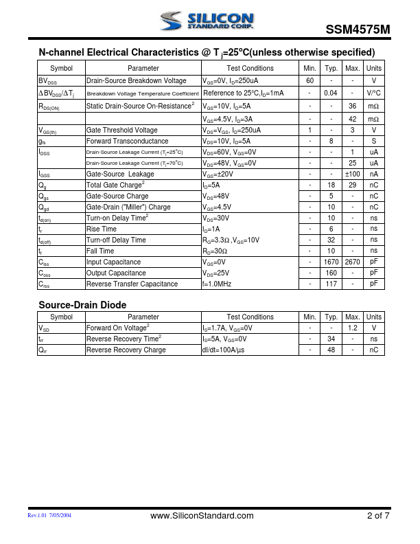
@ T j=25oC(unless otherwise specified) Symbol BVDSS Parameter Drain-Source Breakdown Voltage Test Conditions VGS=0V, ID=250uA Min. 60 1 Typ. 0.04 8 18 5 10 10 6 32 10 160 117 Max. Silicon Standard