2N5452
Overview
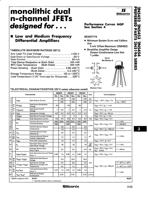
monolithic dual n-channel JFETs designed for • • • H Siliconix Performance Curves NQP See Section 4 • Low and Medium Frequency DiHerential Amplifiers BENEFITS • Minimum System Error and Calibration...
| Part | 2N5452 |
|---|---|
| Description | monolithic dual n-channel JFET |
| Manufacturer | Siliconix |
| Size | 83.74 KB |
monolithic dual n-channel JFETs designed for • • • H Siliconix Performance Curves NQP See Section 4 • Low and Medium Frequency DiHerential Amplifiers BENEFITS • Minimum System Error and Calibration...
| Part Number | Manufacturer | Description |
|---|---|---|
| 2N5452 | Intersil | DUAL N-CHANNEL JFET |
| 2N5457 | Motorola Semiconductor | GENERAL PURPOSE JFET |
| 2N5459 | Motorola Semiconductor | GENERAL PURPOSE JFET |
| 2N5459 | Fairchild Semiconductor | N-Channel General Purpose Amplifier |
| 2N5453 | Intersil | DUAL N-CHANNEL JFET |