The following content is an automatically extracted verbatim text
from the original manufacturer datasheet and is provided for reference purposes only.
View original datasheet text
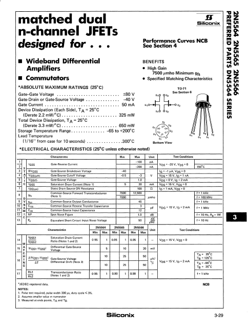
matched dual n-channel JFETs
designed for • • •
H
Siliccnix
Performance Curves NCB See Section 4
• Wideband Differential Amplifiers
• Commutators
BENEFITS
• High Gain 7500 ~mho Minimum 9fs
• Specified Matching Characteristics
*ABSOLUTE MAXIMUM RATINGS (25°C)
Gate-Gate Voltage .......................... ±80V
Gate·Drain or Gate·Source Voltage .............. -40 V Gate Current ............................... 50mA Device Dissipation (Each Side), T A = 25°C
(Derate 2.2 mW;oC) ....................... 325mW Total Device Dissipation, T A = 25°C
(Derate 3.3 mW;oC) ..............•........ 650mW Storage Temperature Range .............. -65 to +200°C Lead Temperature
(1/16" from case for 10 seconds) ...............300°C
TO·71
See Section 6
~~G, G2 8, 52
82
G, 30 o·o.