E400
monolithic dual n-channel JFETs designed for
- -
- - FEr Input Amplifiers
- Low and Medium Frequency
Amplifiers
- Impedance Converters
Hm oo~
Performance Curves NQP See Section 4
BENEFITS m
-o ~
- Minimum System Error and Calibration
10 m V Offset Maximum (E400,
E401)
80 d B Typical CMRR
- Low Drift with Temperature 10/Nrc (E400)
- Simplifies Amplifier Design
Output Conductance < 10 Ilmho
ABSOLUTE MAXIMUM RATINGS (25°C) Gate-To-Gate Voltage _______ ±40 V Gate-Drain or Gate-Source Voltage -40 V Gate Cu rrent
- . SOm A Total Package Dissipation
(25°C Free-Air Temperature) _ 3S0m W Power Derating (to +12Soc). _.... 3.S m Wr C Storage Temperature Range -S5 to +125°C Operating Temperature Range -55 to +125°C Lead Temperature
(1/16" from case for 10 seconds) _. 300°C
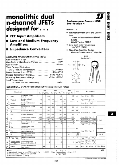
Si- 200 See Section 5
~~ rrr:~
G,
G2
5,
S2 s, 0,
° G,
04 560
032 10
G1...