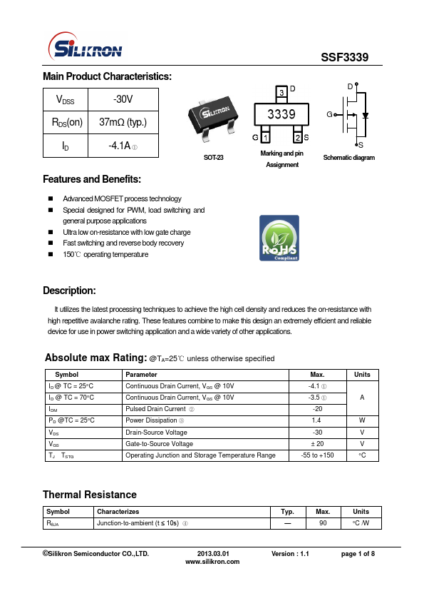
SSF3339
SSF3339 is MOSFET manufactured by Silikron Semiconductor.
Features and Benefits:
- Advanced MOSFET process technology
- Special designed for PWM, load switching and general purpose applications
- Ultra low on-resistance with low gate charge
- Fast switching and reverse body recovery
- 150℃ operating temperature
Marking and pin Assignment
Schematic diagram
Description
:
It utilizes the latest processing techniques to achieve the high cell density and reduces the on-resistance with high repetitive avalanche rating. These features bine to make this design an extremely efficient and reliable device for use in power switching application and a wide variety of other applications.
Absolute max Rating: @TA=25℃ unless otherwise specified
Symbol ID @ TC = 25°C ID @ TC = 70°C IDM PD @TC = 25°C VDS VGS TJ TSTG
Parameter Continuous Drain Current, VGS @ 10V Continuous Drain Current, VGS @ 10V Pulsed Drain Current ② Power Dissipation ③ Drain-Source Voltage Gate-to-Source Voltage Operating Junction and Storage Temperature Range
Max. -4.1 ① -3.5 ①
-20 1.4 -30 ± 20 -55 to +150
Units
W V V °C
Thermal Resistance
Symbol RθJA
Characterizes Junction-to-ambient (t ≤ 10s) ④
©Silikron Semiconductor CO.,LTD.
2013.03.01 .silikron.
Typ.
- Max. 90
Units °C /W
Version : 1.1 page 1 of 8
Electrical Characterizes @TA=25℃ unless otherwise specified
Symbol Parameter V(BR)DSS Drain-to-Source breakdown voltage
RDS(on) Static Drain-to-Source on-resistance
VGS(th) Gate threshold voltage
IDSS Drain-to-Source leakage current
IGSS Gate-to-Source forward leakage
Qg Total gate charge
Qgs Gate-to-Source charge
Qgd Gate-to-Drain("Miller") charge td(on)
Turn-on delay time tr Rise time td(off)
Turn-Off delay time tf Fall...