2N7002K2
Features and Benefits:
- Advanced trench MOSFET process technology
- Special designed for PWM, load switching and general purpose applications
- Ultra low on-resistance with low gate charge
- High Power and current handing capability
- Fully Avalanche Rated
- ESD Protection HBM ≥ 2KV
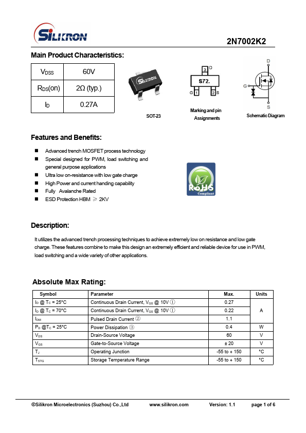
Marking and pin Assignments
Schematic Diagram
Description
:
It utilizes the advanced trench processing techniques to achieve extremely low on resistance and low gate charge. These features bine to make this design an extremely efficient and reliable device for use in PWM, load switching and a wide variety of other applications.
Absolute Max Rating:
Symbol ID @ TC = 25°C ID @ TC = 70°C IDM PD @TC = 25°C VDS VGS TJ TSTG
Parameter
Continuous Drain Current, VGS @ 10V ① Continuous Drain Current, VGS @ 10V ① Pulsed Drain Current ② Power Dissipation ③
Drain-Source Voltage Gate-to-Source Voltage Operating Junction Storage Temperature Range
Max. 0.27 0.22 1.1 0.4 60 ± 20 -55 to + 150 -55 to +...