SMI120N32E2
Features and Benefits:
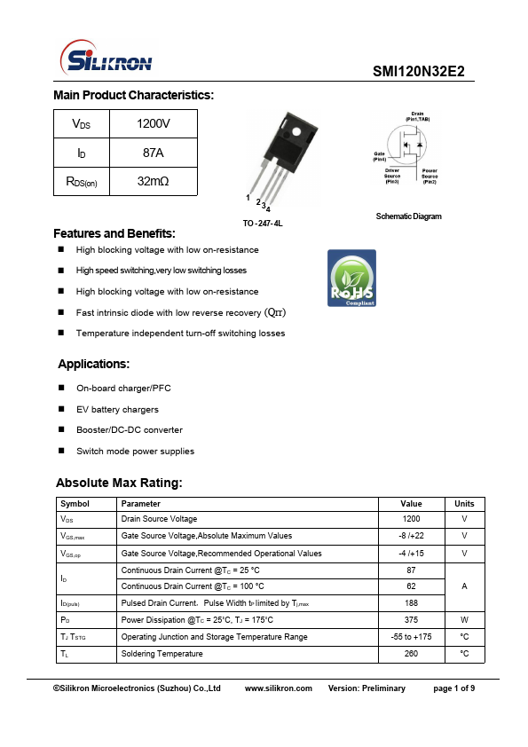
- 247- 4L
- High blocking voltage with low on-resistance
- High speed switching,very low switching losses
- High blocking voltage with low on-resistance
- Fast intrinsic diode with low reverse recovery (Qrr)
- Temperature independent turn-off switching losses
Applications:
- On-board charger/PFC
- EV battery chargers
- Booster/DC-DC converter
- Switch mode power supplies
Absolute Max Rating:
Symbol VDS VGS,max VGS,op
ID(puls) PD TJ TSTG TL
Parameter Drain Source Voltage Gate Source Voltage,Absolute Maximum Values Gate Source Voltage,Remended Operational Values Continuous Drain Current @TC = 25 °C Continuous Drain Current @TC = 100 °C Pulsed Drain Current,Pulse Width t P limited by Tj,max Power Dissipation @TC = 25˚C, TJ = 175˚C Operating Junction and Storage Temperature Range Soldering Temperature
Schematic Diagram
Value 1200 -8 /+22 -4 /+15
87 62 188 375 -55 to +175 260
Units V V V
W °C °C
©Silikron Microelectronics (Suzhou)...