SSF6808J73X
Features and Benefits:
- Advanced MOSFET process technology
- Special designed for PWM, load switching and general purpose applications
- Ultra low on-resistance with low gate charge
- Fast switching and reverse body recovery
- 150℃ operating temperature
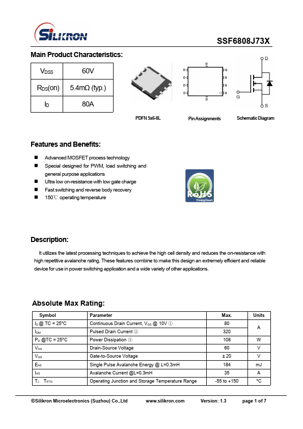
Pin Assignments
Schematic Diagram
Description
:
It utilizes the latest processing techniques to achieve the high cell density and reduces the on-resistance with high repetitive avalanche rating. These features bine to make this design an extremely efficient and reliable device for use in power switching application and a wide variety of other applications.
Absolute Max Rating:
Symbol ID @ TC = 25°C IDM PD @TC = 25°C VDS VGS EAS IAS TJ TSTG
Parameter Continuous Drain Current, VGS @ 10V ① Pulsed Drain Current ② Power Dissipation ③ Drain-Source Voltage Gate-to-Source Voltage Single Pulse Avalanche Energy @ L=0.3m H Avalanche Current @L=0.3m H Operating Junction and Storage Temperature Range
Max. 80 320 108 60 ± 20 184...