DESCRIPTION
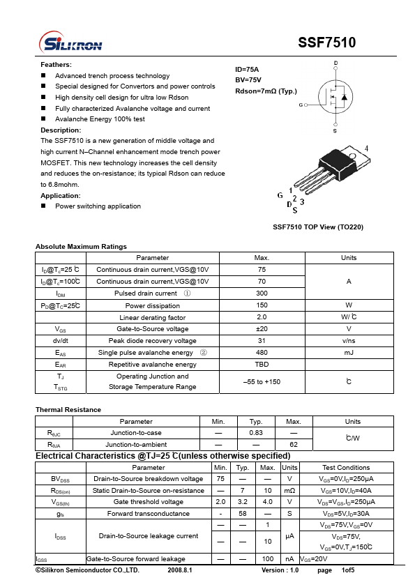
: Application: Power switching application ID=75A BV=75V Rdson=7mΩ (Typ.) ABSOLUTE MAXIMUM RATINGS
Parameter ID@Tc=25 ْC Continuous drain current,VGS@10V ID@Tc=100ْC IDM Continuous drain current,VGS@10V Pulsed drain current ① PD@TC=25ْC Power dissipation Linear derating factor VGS dv/dt Gate-to-Source voltage Peak diode recovery voltage EAS Single pulse avalanche energy ② EAR TJ TSTG Repetitive avalanche energy Operating Junction and Storage Temperature Range SSF7510 TOP View (TO220) Max. 75 70 300 150 2.0 ±20 31 480 TBD –55 to +150 Units A W W/ ْC V v/ns mJ ْC Thermal Resistance Parameter Min. Typ. Max. Units RθJC Junction-to-case — 0.83 — RθJA Junction-to-ambient — — 62 ELECTRICAL CHARACTERISTICS
@TJ=25 ْC(unless otherwise specified) ْC/W Parameter Min. Typ. Max. Units Test Conditions BVDSS RDS(on) VGS(th) gfs IDSS Drain-to-Source breakdown voltage 75 — Static Drain-to-Source on-resistance — 7 Gate threshold voltage 2.0 3.2 Forward transconductance - 58 —— Drain-to-Source leakage current —— IGSS Gate-to-Source forward leakage ©Silikron Semiconductor CO.,LTD. Silikron