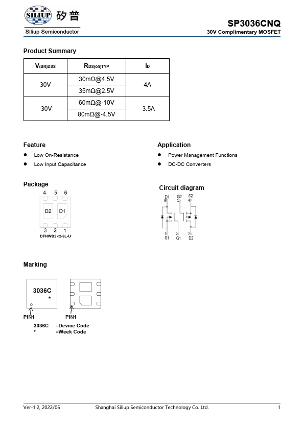
The following content is an automatically extracted verbatim text
from the original manufacturer datasheet and is provided for reference purposes only.
View original datasheet text
Product Summary
V(BR)DSS 30V -30V
RDS(on)TYP 30mΩ@4.5V 35mΩ@2.5V 60mΩ@-10V 80mΩ@-4.5V
ID 4A -3.5A
SP3036CNQ
30V Complimentary MOSFET
Feature
Low On-Resistance Low Input Capacitance
Package
Application
Power Management Functions DC-DC Converters
Circuit diagram
DFNWB2×2-6L-U
Marking
PIN1
3036C *
PIN1
=Device Code =Week Code
Ver-1.2, 2022/06
Shanghai Siliup Semiconductor Technology Co. Ltd.
1
SP3036CNQ
30V Complimentary MOSFET
Absolute maximum ratings (Ta=25℃ unless otherwise noted)
Parameter
Symbol
N-Channel
P-Channel
Unit
Drain-Source Voltage
VDS
Gate-Source Voltage
VGS
Continuous Drain Current1
ID
Pulsed Drain Current
IDM
Maximum Power Dissipation
PD
Thermal Resistance from Junction to Ambient(t≤5s)
RθJA
30
-30
±20
±20
4
-3.5
12
-10
2
62.