SP6260
SP6260 is Extremely Low Noise 150mA LDO Regulator manufactured by Sipex.
features g g g g g g g g g g g g Low Dropout Voltage at IOUT=100m A: 150m V Typical (Except 1.5V Version) Low Standby Current: 0.1PA Typical Low Quiescent Current: 25PA Typical High Ripple Rejection: 70d B Typical˄f=10k Hz˅ Maximum Output Current: More Than 150m A (300m A Limit) Extremely Low Noise: 30PVrms (10Hz to 100k Hz) Excellent Line Regulation: 4m V Typical Excellent Load Regulation: 12m V Typical High Output Voltage Accuracy: r2% Excellent Line Transient Response and Load Transient Response patible with Low ESR Ceramic Capacitor (as Low as 1PF) Available in Lead Free, Ro HS pliant Package: SOT-23-5 SOT-2-5 Package
VIN GND CE
2
VOUT
Applications g g g g g g Mobile Phones, Cordless Phones Wireless munication Equipment Portable Games Cameras, Video Recorders Sub-board Power Supplies for Tele Equipment Battery Powered Equipment
DESCRIPTION
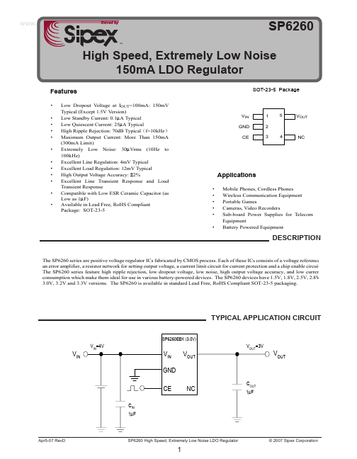
The SP6260 series are positive voltage regulator ICs fabricated by CMOS process. Each of these ICs consists of a voltage reference, an error amplifier, a resistor network for setting output voltage, a current limit circuit for current protection and a chip enable circuit. The SP6260 series feature high ripple rejection, low dropout voltage, low noise, high output voltage accuracy, and low current consumption which make them ideal for use in various battery-powered devices. The SP6260 devices have 1.5V, 1.8V, 2.5V, 2.8V, 3.0V, 3.2V and 3.3V versions. The SP6260 is available in standard Lead Free, Ro HS pliant SOT-23-5 packaging.
TYPICAL APPLICATION CIRCUIT
SP6260EEK (.0V)
VIN=V
VIN GND CE
CIN PF
VOUT
VOUT=V
VOUT
COUT PF
Apr5-07 Rev D
SP6260 High Speed, Extremely Low Noise LDO Regulator
© 2007 Sipex Corporation
AP2121 Pin Configuration
Package Pinout (SOT-2-5)
VIN GND CE
2
VOUT
SOT-2-5
Package Perspective of SOT2-5
Pin Configuration of SP6260 (Top View)
Pin Description
Pin Number 1 2 3 4 5 Pin Name VIN GND CE NC VOUT Input voltage Ground Active high enable input pin....