SBL3030CT
SBL3030CT is Low VF Schottky Barrier Rectifiers manufactured by Sirectifier.
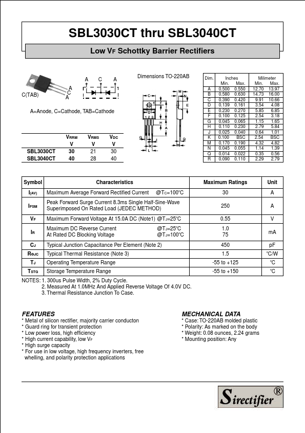
SBL3030CT thru SBL3040CT
Low VF Schottky Barrier Rectifiers
C(TAB)
AC A
A=Anode, C=Cathode, TAB=Cathode
SBL3030CT SBL3040CT
VRRM V 30 40
VRMS V 21 28
VDC V 30 40
Dimensions TO-220AB
Dim.
A B C D E F G H J K M N Q R
Inches Min. Max. 0.500 0.550 0.580 0.630 0.390 0.420 0.139 0.161 0.230 0.270 0.100 0.125 0.045 0.065 0.110 0.230 0.025 0.040 0.100 BSC 0.170 0.190 0.045 0.055 0.014 0.022 0.090 0.110
Milimeter Min. Max. 12.70 13.97 14.73 16.00 9.91 10.66 3.54 4.08 5.85 6.85 2.54 3.18 1.15 1.65 2.79 5.84 0.64 1.01 2.54 BSC 4.32 4.82 1.14 1.39 0.35 0.56 2.29 2.79
Symbol
Characteristics
I(AV) Maximum Average Forward Rectified Current @TC=100oC
IFSM
Peak Forward Surge Current...