Overview: STPR2010CT thru STPR2020CT
Ultra Fast Recovery Diodes
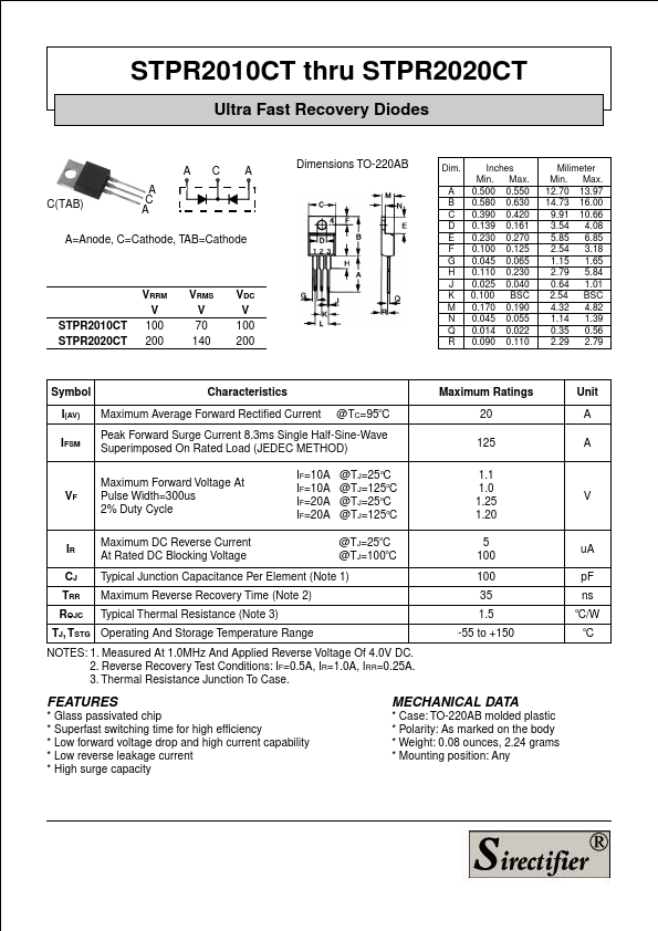
 C(TAB) AC A
A C A A=Anode, C=Cathode, TAB=Cathode STPR2010CT STPR2020CT VRRM V
100 200 VRMS V 70
140 VDC V
100 200 Dimensions TO-220AB Dim.
A B C D E F G H J K M N Q R Inches Min. Max. 0.500 0.550 0.580 0.630 0.390 0.420 0.139 0.161 0.230 0.270 0.100 0.125 0.045 0.065 0.110 0.230 0.025 0.040 0.100 BSC 0.170 0.190 0.045 0.055 0.014 0.022 0.090 0.110 Milimeter Min. Max. 12.70 13.97 14.73 16.00 9.91 10.66 3.54 4.08 5.85 6.85 2.54 3.18 1.15 1.65 2.79 5.84 0.64 1.01 2.54 BSC 4.32 4.82 1.14 1.39 0.35 0.56 2.29 2.79 Symbol Characteristics I(AV) Maximum Average Forward Rectified Current @TC=95oC
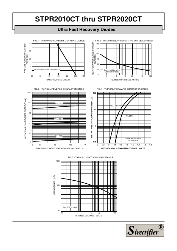
 IFSM Peak Forward Surge Current 8.3ms Single Half-Sine-Wave Superimposed On Rated Load (JEDEC METHOD) Maximum Ratings 20
125 Unit A
A Maximum Forward Voltage At VF Pulse Width=300us
2% Duty Cycle IF=10A IF=10A IF=20A IF=20A @TJ=25oC @TJ=125oC @TJ=25oC @TJ=125oC 1.1 1.0 1.25 1.20 V IR Maximum DC Reverse Current At Rated DC Blocking Voltage @TJ=25oC @TJ=100oC 5 100 CJ Typical Junction Capacitance Per Element (Note 1) TRR Maximum Reverse Recovery Time (Note 2) ROJC Typical Thermal Resistance (Note 3) TJ, TSTG Operating And Storage Temperature Range 100 35 1.5 -55 to +150 NOTES: 1. Measured At 1.0MHz And Applied Reverse Voltage Of 4.0V DC. 2. Reverse Recovery Test Conditions: IF=0.5A, IR=1.0A, IRR=0.25A. 3. Thermal Resistance Junction To Case.