SKY65015-92LF
SKY65015-92LF is InGaP Cascable AMplifier manufactured by Skyworks Solutions.
Features
- -
- -
- -
- -
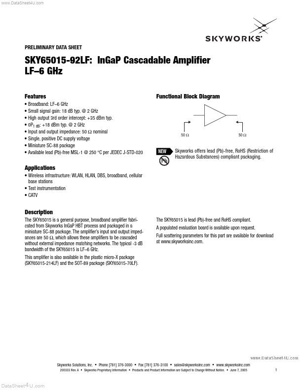
Functional Block Diagram
Broadband: LF- 6 GHz Small signal gain: 18 d B typ. @ 2 GHz High output 3rd order intercept: +35 d Bm typ. 0P1 d B: +18 d Bm typ. @ 2 GHz Input and output impedance: 50 Ω nominal Single, positive DC supply voltage Miniature SC-88 package Available lead (Pb)-free MSL-1 @ 250 °C per JEDEC J-STD-020
50 Ω
50 Ω
Skyworks offers lead (Pb)-free, Ro HS (Restriction of Hazardous Substances) pliant packaging.
Applications
- -
- Wireless infrastructure: WLAN, HLAN, DBS, broadband, cellular base stations Test instrumentation CATV
Description
The SKY65015 is a general purpose, broadband amplifier fabricated from Skyworks In Ga P HBT process and packaged in a miniature SC-88 package. The amplifier’s input and output impedances are 50 Ω, which allows these amplifiers to be cascaded without external impedance matching networks. The typical -3 d B bandwidth of the SKY65015 is LF- 6 GHz. This amplifier is also available in the plastic micro-X package (SKY65015-214LF) and the SOT-89 package (SKY65015-70LF). The SKY65015 is lead (Pb)-free and Ro HS pliant. A populated evaluation board is available upon request. Full scattering parameters for this part are available for download at .skyworksinc..
Skyworks Solutions, Inc.
- Phone [781] 376-3000
- Fax [781] 376-3100
- sales@skyworksinc.
- .skyworksinc.
200333 Rev. A
- Skyworks Proprietary Information
- Products and Product Information are Subject to Change Without Notice.
- June 7, 2005
Data Sheet 4 U .
..
PRELIMINARY DATA SHEET
- SKY65015-92LF
Electrical Specifications at 25 °C
T = 25 °C, IS = 70 m A, PIN = 0 d Bm, Z0 = 50 Ω, measured in evaluation board, unless otherwise noted
Parameter Small signal gain 3 d B gain bandwidth Noise figure Output power at 1 d B pression Input and output VSWR Output third order intercept point Operating voltage Reverse isolation Gain flatness Thermal resistance θJC Symbol GP BW NF 0P1 d B VSWR OIP3 VD |s12| PIN = 0 d Bm each tone, ∆f = 10 MHz Measured...