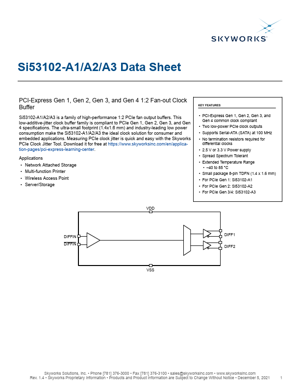
Download Si53102-A3 Datasheet PDF
Si53102-A3 page 2
Page 2
Si53102-A3 page 3
Page 3

Si53102-A3 Description

This low-additive-jitter clock buffer family is pliant to PCIe Gen 1, Gen 2, Gen 3, and Gen 4 specifications. The ultra-small footprint (1.4x1.6 mm) and industry-leading low power consumption make the Si53102-A1/A2/A3 the ideal clock solution for consumer and embedded applications. Measuring PCIe clock jitter is quick and easy with the Skyworks PCIe Clock Jitter Tool.

Si53102-A3 Key Features

  • PCI-Express Gen 1, Gen 2, Gen 3, and Gen 4 mon clock pliant
  • Two low-power PCIe clock outputs
  • Supports Serial-ATA (SATA) at 100 MHz
  • 2.5 V or 3.3 V Power supply
  • Spread Spectrum Tolerant
  • Extended Temperature Range
  • 40 to 85 °C
  • Small package 8-pin TDFN (1.4 x 1.6 mm)
  • For PCIe Gen 1: Si53102-A1
  • For PCIe Gen 2: Si53102-A2