SL90P02Q
SL90P02Q is P-CHANNEL MOSFET manufactured by Slkor Micro Semicon.
Features
- VDS =-20V,ID =-90A RDS(ON) <2.3 mΩ @ VGS=-10V RDS(ON) <2.6 mΩ @ VGS=-4.5V
- Improved dv/dt capability
- Fast switching
- Good stability and uniformity with high EAS
- Excellent package for good heat dissipation
Applications
- Power switching application
- Networking
- Notebook
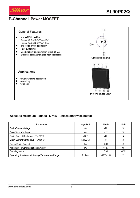
Schematic diagram DFN5X6-8L top view
Absolute Maximum Ratings (TC=25℃unless otherwise noted)
Parameter
Drain-Source Voltage Gate-Source Voltage Drain Current-Continuous (TC=25℃) Drain Current-Continuous (TC=100℃)
Pulsed Drain Current Maximum Power Dissipation (TC=25℃) Derating factor
Operating Junction and Storage Temperature Range
Symbol VDS VGS
ID(25℃)
ID (100℃)
IDM PD
TJ,TSTG
Limit
-20 ±12 -90 -54 -360 41.67 0.33 -55 To 150
Unit
A W W/℃ ℃
.slkormicro.
Thermal Characteristic
Thermal Resistance,Junction-to-Case(Note 2)
RθJC
Electrical Characteristics (TC=25℃unless otherwise...