CXL1503M
CXL1503M is CMOS-CCD Signal Processor manufactured by Sony Semiconductor Solutions.
Description
CXL1503M/1505M are CMOS-CCD signal processors developed for CCD camera plementary color filter array processing system. CXL1503M 1H × 4 301.5 bit CCD delay line CXL1505M 1H × 4 453.5 bit CCD delay line Features
- Single power supply 5V
- Low power consumption CXL1503M 100m W (Typ.) CXL1505M 150m W (Typ.)
- Built-in peripheral circuits
- Built-in CDS (Correlated Double Sampling) circuit Function
- Clock driver
- Autobias circuit (center and black)
- Pedestal clamp circuit
- CDS circuit Structure CMOS-CCD Absolute Maximum Ratings (Ta = 25°C) 6 V
- Supply voltage VDD
- Operating temperature Topr
- 10 to +60 °C
- Storage temperature Tstg
- 55 to +150 °C
- Allowable power dissipation PD 500 m W Remended Operating Conditions (Ta = 25°C) Supply voltage VDD 5 ± 5% V Remended Clock Conditions (Ta = 25°C) Item Clock voltage Low Clock voltage High CXL1503M Clock frequency CXL1505M f CL 7.16 MHz Symbol VL VH f CL Min. 0 VDD
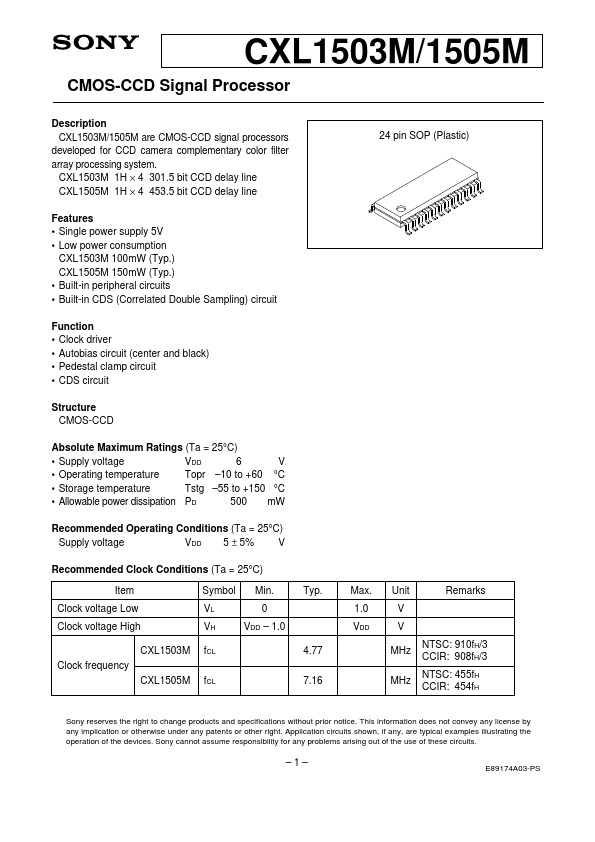
- 1.0 4.77 Typ. Max. 1.0 VDD Unit V V MHz NTSC: 910f H/3 CCIR: 908f H/3 NTSC: 455f H CCIR: 454f H Remarks 24 pin SOP (Plastic)
Sony reserves the right to change products and specifications without prior notice. This information does not convey any license by any implication or otherwise under any patents or other right. Application circuits shown, if any, are typical examples illustrating the operation of the devices. Sony cannot assume responsibility for any problems arising out of the use of these circuits.
- 1-
E89174A03-PS
CXL1503M/1505M
Block Diagram
XDL1 XDL2 VDD VDD VSS VDD VSS
19 ABCN 21 A. B CENTER TIMING GENERATOR ABBL 3 DCAB 23 5V IN A 22 CLP DL A A. B BLACK P. D P. D PG GEN. CDS-OUTPUT CIRCUIT PG GEN. IN B 24 CLP DL B PG GEN. IN C 2 CLP DL C CDS-OUTPUT CIRCUIT PG GEN. IN D 6 CLP DL D CDS-OUTPUT CIRCUIT 9 OUT D 11 OUT C CDS-OUTPUT CIRCUIT 13 OUT B 15 OUT A 18 4 8 1 16 20 17
Pin Configuration (Top View)
VSS 1 IN C 2 ABBL 3 VDD 4 IS 5 IN D 6 CLP 7 VDD 8 OUT D 9 VGG 10 OUT C 11 N.C. 12
24 IN B 23 DCAB 22 IN A 21 ABCN 20 VDD 19 XDL1 18...