CXL5520M
CXL5520M is CMOS-CCD Baseband 1H Delay Line manufactured by Sony Semiconductor Solutions.
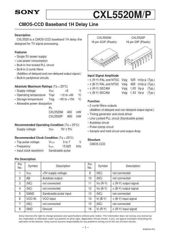
CXL5520M/P
CMOS-CCD Baseband 1H Delay Line
Description CXL5520 is a CMOS-CCD baseband 1H delay line designed for TV signal processing. Features
- Single 5V power supply
- Low power consumption
- Built-in line locked PLL circuit
- Built-in 2 b filters (Addition of delayed and non-delayed output signal.)
- Built-in peripheral circuits...