Sony CDX1250M
This information does not convey any license by any implication or otherwise under any patents or other right.| Part No. | CDX1250M |
|---|---|
| Datasheet | CDX1250M Download |
| Manufacturer |  Sony |
| Description | Vertical Clock Driver for CCD Image sensor |
| Buy | Stock & Price |
DESCRIPTION
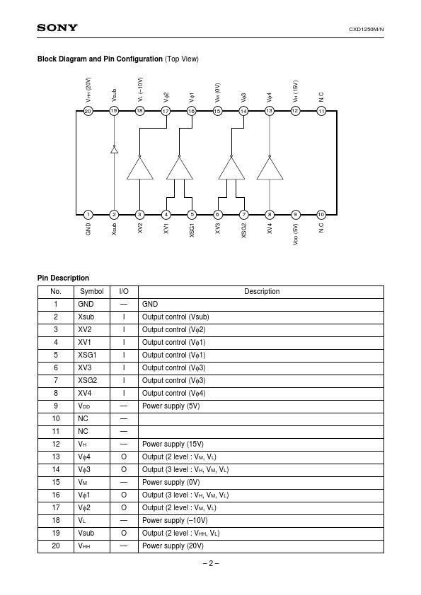
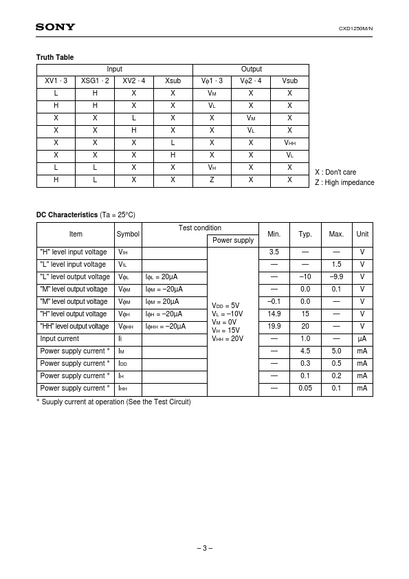
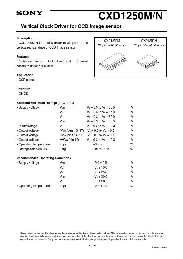
CXD1250M/N is a clock driver developed for the vertical register drive of CCD Image sensor.FEATURES
4-channel vertical clock driver and 1 channel substrate driver are built-in. Application CCD camera Structure CMOSABSOLUTE MAXIMUM RATINGS
(Ta = 25°C)● Supply voltage VDD VM VH VHH
● Input volltage VI
● Output voltage MVφ (pins 13, 17)
● Output voltage HVφ (pins 14, 16)
● Output voltage HHVφ (pin 19)
● Operating temperature Topr
● Storage temperature Tstg Recommended Operating Conditions
● Supply voltage VDD VM VH VHH VL
● Operating temperature Topr CXD1250M 20 pin SOP (Plastic) CXD1250N 20 pin SSOP (Plastic) VL – 0.3 to VL + 35.0 VL – 0.3 to VL + 35.0 VL – 0.3 to VL + 35.0 VL – 0.3 to VL + 35.0 VL – 0.3 to VDD + 0.3 VL – 0.3 to VM + 0.3 VL – 0.3 to VH + 0.3 VL – 0.3 to VHH + 0.3 –25 to +85 –40 to +125 V V V V V V V V °C °C 5.0 ± 0.5 VL + 10.0 VL + 25.0 VL + 30.0 –10.0 –20 to +75 V V V V V °C Sony reserves the right to change products and specifications without prior notice.