Sony CXG1063TN
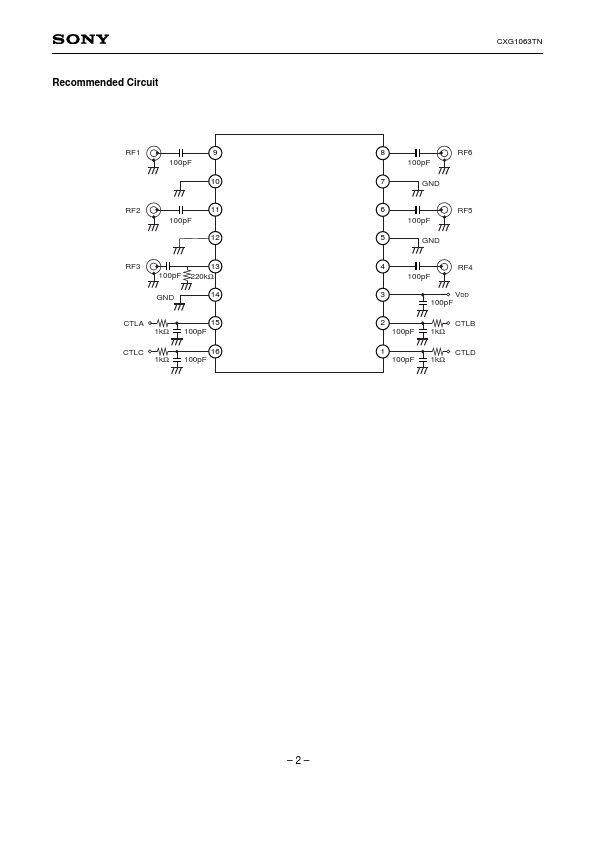
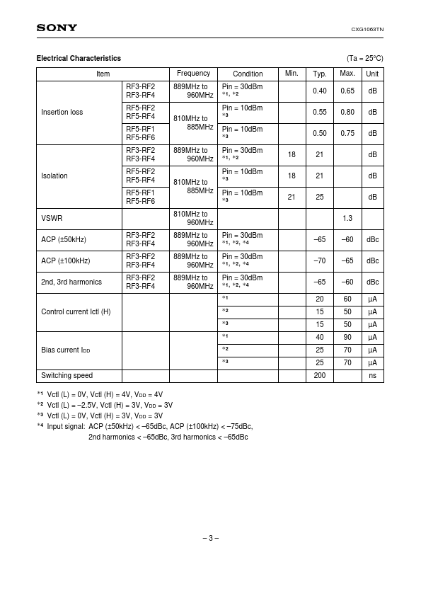
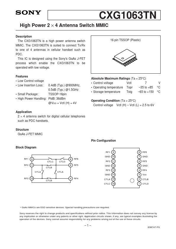
The CXG1063TN is a high power antenna switch MMIC. The CXG1063TN is suited to connect Tx/Rx to one of 4 antennas in cellular handset such as PDC. This IC is designed using the Sony's GaAs J-FET process which enable the CXG1063TN to be operated with low voltage.| Part No. | CXG1063TN |
|---|---|
| Datasheet | CXG1063TN Download |
| Manufacturer |  Sony |
| Description | High Power Antenna Switch MMIC |
| Buy | Stock & Price |
DESCRIPTION
FEATURES
● Low Control voltage● Low Insertion Loss: 16 pin TSSOP (Plastic) 0.4dB (Typ.) @900MHz, 0.5dB (Typ.) @1.5GHz
● Small Package: TSSOP-16pin
● High Power Handling: PldB: 36dBm @VDD = Vctl (H) = 4V Application 2 × 4 antenna switch for digital cellular telephones such as PDC handsets. Structure GaAs J-FET MMIC
ABSOLUTE MAXIMUM RATINGS
(Ta = 25°C)● Control voltage Vctl 7
● Operating temperature Topr –35 to +85
● Storage temperature Tstg –65 to +150 Operating Condition (Ta = 25°C) Control voltage Vctl (H) – Vctl (L) = 2.5 to 6V V °C °C Pin Configuration Block Diagram RF1 RF1 9 CTLC RF2 11 CTLB CTLA RF3 13 CTLB CTLA 4 RF4 CTLD 6 RF5 8 RF6 9 8 7 6 5 4 3 2 1 RF6 GND RF5 GND RF4 VDD CTLB CTLD GND 10 RF2 11 GND 12 RF3 13 GND 14 CTLA 15 CTLC 16
● GaAs MMICs are ESD sensitive devices. Special handling precautions are required. Sony reserves the right to change products and specifications without prior notice. This information does not convey any license by any implication or otherwise under any patents or other right.